36
Table 54 (Continued)
Item
Number
Symptom
Possible cause
9
No transmit(TX)
a. Defective PTT switch
b. Defective regulators IC15 (5V), IC17
(8V)
c. Defective Q32 (TX +B)
d. Check power transmit circuit (Q3, Q4,
IC1)
e. Failure of VCO circuit (Q15 and/or
Q17) or PLL (IC9)
f. Check PLL control voltage for 3.5
VDC at TP1 or channel 16
g. Failure of talk detection circuit (Q9)
[CPU AF Board]
10
Low RF power output
a. Check RF power output from IC1. If
it checks good, check the triple P type
network component (L1, L2, C3, etc.)
and antenna switching diode (D2). If not
good then check the voltage level
outputs of the drive amplifiers Q3 and
Q4 as well the associated circuitry
b. Check power control circuit (Q1, Q2,
Q5) and IC2
11
Poor or no modulation
a. Check VCO output frequency at pin8
of PLL10. PLL phase detector output at
pin 5 of PLL IC9a associated circuitry
b. Check 12.8MHz crystal (XTAL1)
12
PLL output frequency or
incorrect
a. Check frequency of 12.8MHz crystal
(XTAL1)
b. Check the frequency input at pin 8 or
IC9 and verify the transmit frequency
Summary of Contents for RAY 210VHF
Page 2: ......
Page 3: ......
Page 4: ......
Page 6: ......
Page 8: ......
Page 10: ......
Page 12: ......
Page 19: ...7 Figure 2 2 Outline and Mounting Dimensions...
Page 30: ...18 Figure 3 1 Layout of Controls and Connectors...
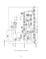
Page 40: ...28 Fig 4 1 Block Diagram RF PCB...
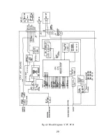
Page 41: ...29 Fig 4 2 Block Diagram CPU PCB...
Page 55: ...43 6 2 RAY210 ASSEMBLY DRAWING...
Page 57: ...45 6 3 SCHEMATIC DIAGRAM Fig 6 1 Schematic diagram RF PCB...
Page 58: ...46 Fig 6 2 Schematic diagram CPU PCB l...
Page 59: ...47 Fig 6 2 Schematic diagram CPU PCB 2...
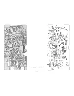
Page 60: ...48 Fig 6 3 RF PCB Layout Top View...
Page 61: ...49 Fig 6 4 RF PCB Layout Rear View...
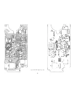
Page 62: ...50 Fig 6 5 CPU PCB Layout Top view...
Page 63: ...51 Fig 6 5 CPU PCB Layout Rear View...
Page 64: ...52...
Page 75: ...63...


