PDP-5050SX
213
5
6
7
8
5
6
7
8
C
D
F
A
B
E
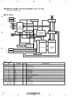
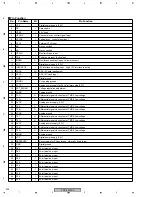
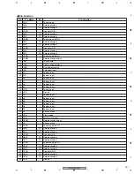
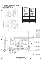
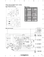
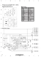
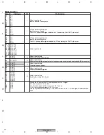
No.
Pin Name
I/O
Pin Function
7
14
21
28
S-1
S-2
S-3
S-4
−
Composite video/S selector.
The detection results are written to the status register.
S signal at 3.5 V or less. Composite video signal at 3.5 V or more.
This pin is pulled up to 5 V by a 100 k ohm resistor, so the composite video signal is selected when
open.
32
ADR
−
Selects the slave address for the I2C bus.
90H at 1.5 V or less 92H at 2.5 V or more 90H when open.
33
SCL
I
I2C bus signal input VILmax=1.5 V VIHmin=3.0 V
34
SDA
I
I2C bus signal input VILmax=1.5 V VIHmin=3.0 V VOLmax=0.4 V
36
DC_OUT
O
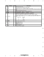
Outputs the S2-compatible DC superimposed onto the COUT3 output.
The DC is superimposed by connecting this pin to the COUT3 output via a capacitor.
Control is performed by the I2C bus. When 0 V is output, Q1 is ON and the impedance is 5 k ohm.
S2 protocol output impedance of 10
±
3 k ohm is realized by attaching external resistance of 4.7 k
ohm.
DC_OUT (bus)
Output DC
0
4.5 V
1
0 V
2
1.9 V
3
4.5 V
55
46
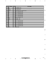
TRAP1
TRAP2
−
Connects trap circuit for subcarrier.
48
MUTE
−
Audio signal output mute.
Mute OFF at 1.5 V or less
Mute ON at 2.5 V or more
Mute OFF when open.
50
BIAS
−
Internal reference bias (VCC/2).
Connect to GND via a capacitor.

