background image

PDP-5050SX

125

5

6

7

8

5

6

7

8

C

D

F

A

B

E

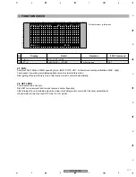
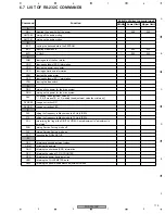
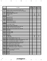
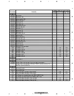
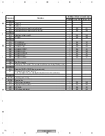
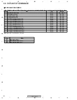
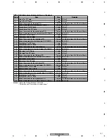
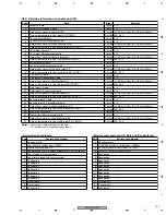
GS1: Returning information on the model and the version of the software

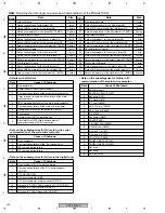
GPM: Returning the data of the PDP pulse meter

Breakdown of the data on the display

Order

Data

Size

1

Data on the display

3 bytes

2

Version of the module microcomputer

4 bytes

3

Version of the IC4-MANTA

4 bytes

4

Sequence version (50VIDEO)

4 bytes

5

Sequence version (50PC)

4 bytes

6

Sequence version (43VIDEO)

4 bytes

7

Sequence version (43PC)

4 bytes

8

Version of the IF microcomputer

4 bytes

9

Version of the main microcomputer
boot Software

4 bytes

10

Version of the main microcomputer

4 bytes

11

12

13

14

Version of the IC3 boot Software 

4 bytes

4 bytes

4 bytes

4 bytes

Version of the IC3 Program

Version of the IC3 Enhanced

Version of the IC3 GUI

Order

Data

Size

1

Pulse meter (Block area 1)

10 bytes

2

Pulse meter (Block area 2)

10 bytes

3

Pulse meter (Block area 3)

10 bytes

4

Pulse meter (Block area 4)

10 bytes

5

Pulse meter (Block area 5)

10 bytes

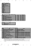
GPC: Returning the cumulative number of times the power to the PDP was turned on

• Commands for clearing the logs

Order

Data

Size

1

Power-on counter

8 bytes

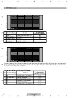
Data

Model

HD5

PDP-5050SX

HD4

PDP-4350SX

Note: Refer to the service manual of the panel.

Parameter

Corresponding

RS-232C Command

PD INFO

CPD

SD1 INFO

CSD

SD2 INFO

CNG

HOUR METER

CHM

PULSE METER

CPM

P ON COUNTER

CPC

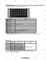
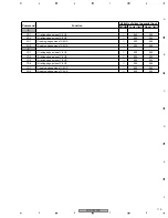
GS6: Returning information of the Flash Device

Order

Data

Size

1

Display Information

3 bytes

2

Version of the CCD UCOM

4 bytes

3

Version of the DTV Software

4 bytes

4

Version of the DTV Hardtware

2 bytes

5

Version of the DTV Hardtware Serial

6bytes

6

Not Used (Reserve)

56 bytes

7

User Password

4 bytes

Summary of Contents for PDP4350SX

Page 1: ...6 PIONEER CORPORATION 2005 PDP 5050SX ARP3261 PLASMA DISPLAY SYSTEM PDP 5050SX PDP 4350SX THIS MANUAL IS APPLICABLE TO THE FOLLOWING MODEL S AND TYPE S This service manual should be used together with the following manual s Model Type Power Requirement Remarks PDP 5050SX KUC AC120V PDP 4350SX KUC AC120V Model No Order No Remarks PDP 5050SX PDP 4350SX ARP3262 SCHEMATIC DIAGRAM PCB CONNECTION DIAGRA...

Page 2: ... adjustment and compartment covershields isolation resistor capacitor etc 3 When service is required observe the original lead dress Extra precaution should be taken to assure correct lead dress in the high voltage circuitry area 4 Always use the manufacture s replacement components Especially critical components as indicated on the circuit diagram should not be replaced by other manufacture s Fur...

Page 3: ...c Any current measured must not exceed 0 5mA ANY MEASUREMENTS NOT WITHIN THE LIMITS OUTLINED ABOVE ARE INDICATIVE OF A POTENTIAL SHOCK HAZARD AND MUST BE CORRECTED BEFORE RETURNING THE SET TO THE CUSTOMER PRODUCT SAFETY NOTICE Many electrical and mechanical parts in PIONEER set have special safety related characteristics These are often not evident from visual inspection nor the protection afforde...

Page 4: ... the charged places described above If the places are touched there is a risk of electric shock 1 PANEL POWER SUPPLY Unit 223V 2 50 X DRIVE Assy 230V to 223V 3 50 Y DRIVE Assy 353V 4 50 SCAN AAssy 353V 5 50 SCAN B Assy 353V 6 X CONNECTOR AAssy 230V to 223V 7 X CONNECTOR B Assy 230V to 223V Part is the High Voltage Generating Points other than the Charged Section Part is Charged Section AC Inlet wi...

Page 5: ... the charged places described above If the places are touched there is a risk of electric shock 1 PANEL POWER SUPPLY Unit 215V 2 43 X DRIVE Assy 235V to 215V 3 43 Y DRIVE Assy 345V 4 43 SCAN AAssy 345V 5 43 SCAN B Assy 345V 6 X CONNECTOR AAssy 235V to 215V 7 X CONNECTOR B Assy 235V to 215V Part is the High Voltage Generating Points other than the Charged Section Part is Charged Section AC Inlet wi...

Page 6: ... the product Please check that neither solder debris nor screws remain inside the product 8 There should be no semi broken wires scratches melting etc on the coating of the power cord Damaged power cords may lead to fire accidents so please be sure that there are no damages If you find a damaged power cord please exchange it with a suitable one 9 There should be no spark traces or similar marks on...

Page 7: ...SSY 48 3 1 7 50 X DRIVE ASSY 49 3 1 8 DIGITAL VIDEO ASSY 50 3 1 9 AV BOARD ASSY 52 3 1 10 MAIN BOARD ASSY 54 3 1 11 AUDIO AMP ASSY 56 3 1 12 MR POWER SUPPLY UNIT 57 3 1 13 TUNER BOARD ASSY 58 3 2 WAVEFORMS 59 3 3 VOLTAGES 65 4 PCB CONNECTION DIAGRAM Refer to Service Manual ARP3262 5 PCB PARTS LIST 71 6 ADJUSTMENT 92 6 1 POSSIBLE CASES WHERE READJUSTMENT IS REQUIRED 92 6 2 DRIVE ASSY ADJUSTMENT 94 ...

Page 8: ...can TV standard NTSC system Circuit type Video signal detection PLL full synchronous detection PLL digital synthesizer system Tuner VHF UHF VHF 2 13ch UHF 14 69ch CATV ANTENNA CABLE A IN 1 135ch Cable 1 125ch Audio multiplex BTSC system Terminals Rear ANTENNA CABLE A IN 75 Ω UNBAL F Type for DTV VHF UHF CATV in ANTENNA B 75 Ω UNBAL F Type for VHF UHF CATV in Loop out INPUT 1 COMPONENT VIDEO in S V...

Page 9: ...PDP 5050SX 9 5 6 7 8 5 6 7 8 C D F A B E ...

Page 10: ... some component parts indicates the importance of the safety factor of the part Therefore when replacing be sure to use parts of identical designation Screws adjacent to mark on product are used for disassembly For the applying amount of lubricants or glue follow the instructions in this manual In the case of no amount instructions apply as you think it appropriate NOTES 8 2 1 13 12 7 10 6 5 4 19 ...

Page 11: ...SP 5 Dry Cell Battery VEM1021 6 Power Cord ADG1215 7 Binder Assy AEC1908 8 Cleanning Cloth AED1208 9 Polyethylene Bag S AHG1338 NSP 10 Catalogue Bag AHG1340 NSP 11 Warranty Card ARY1138 12 DCR User Card ARY1162 NSP 13 User Card VRY1132 14 Pad 50T L AHA2439 15 Pad 50T R AHA2440 16 Pad 50B L AHA2441 17 Pad 50B R AHA2442 18 Accessory Case SX AHC1066 19 Under Carton 5050 AHD3358 20 Upper Carton 5050 A...

Page 12: ...2 22 22 22 19 18 17 22 22 22 9 8 6 4 10 22 22 22 11 7 5 22 21 21 21 2 16 21 21 21 21 21 20 20 21 15 22 25 22 22 22 22 23 24 14 22 20 21 21 3 15 22 20 12 13 Cushions of No 17 18 and 19 cannot be reused once they are peeled off When they are to be removed order new parts The mark is engraved at the attaching point for screw of No 20 ...

Page 13: ... ANG2754 7 Grip R AMR3441 8 Grip L AMR3440 9 Mini Clamp AEC1805 10 Edge Saddle AEC2030 11 Locking Wire Saddle AEC1948 12 Terminal Label POW AAX3186 13 Terminal Label SX AAX3185 14 Terminal Label POD AAX3184 15 Grip Label AAX3188 16 Serial Seal AAX3143 17 Cushion AED1274 18 Cushion AED1273 19 Cushion AED1271 20 Screw ABA1333 21 Screw ABZ30P100FTB 22 Screw AMZ30P060FTB NSP 23 Name Label 5050 AAL2672...

Page 14: ...PDP 5050SX 14 1 2 3 4 1 2 3 4 C D F A B E 2 1 3 FRONT SECTION 2 Refer to 2 1 4 2 1 6 CHASSIS SECTION 1 3 3 3 4 3 2 8 12 13 11 10 8 7 7 6 1 9 5 14 14 16 15 16 16 16 16 15 ...

Page 15: ...0P AMB2823 4 Pioneer Badge AAM1098 NSP 5 SR Lens P AAK2798 NSP 6 Function Button AAC1555 7 Panel Cushion V 50 AED1258 8 Panel Cushion H 50 AED1257 9 Flexible Flat Cable J211 ADD1225 10 Power Button AAD4127 11 Coil Spring ABH1114 NSP 12 LED Lens P AAK2799 13 Blind Cushion AEB1383 14 Panel Holder H Assy 50 ANG2678 15 Panel Holder V 50 ANG2663 16 Screw ABZ30P060FTC ...

Page 16: ... 4 C D F A B E 2 1 4 CHASSIS SECTION 1 3 A A 7 4 4 2 3 1 6 5 27 25 24 24 24 24 27 27 27 27 15 16 27 27 27 17 17 19 26 7 4 19 18 20 17 17 24 24 24 9 25 27 27 27 8 5 27 27 27 27 27 26 11 1 13 14 12 10 24 25 6 3 26 21 21 23 2 23 22 ...

Page 17: ...ont Chassis HD Assy 50 ANA1793 10 Front Chassis HU Assy 50 ANA1792 11 Front Chassis VL 5050 ANA1847 12 Front Chassis VR 5050 ANA1848 13 Sub Frame L Assy 5050 ANG2758 14 Sub Frame R Assy 5050 ANG2759 15 IR Holder ANG2665 16 Locking Wire Saddle AEC1948 17 Wire Saddle AEC1745 18 Toggle Fixer AEC2021 19 PCB Spacer AEC1947 20 Wire Saddle AEC2031 21 Circuit Board Spacer AEC1872 22 Wire Saddle AEC1751 23...

Page 18: ...C D F A B E 2 1 5 CHASSIS SECTION 2 3 A B A B 5 13 12 8 9 11 10 7 6 15 14 16 9 17 6 1 31 31 32 34 35 20 21 19 22 30 30 36 36 8 2 7 23 24 19 35 36 31 25 11 18 26 37 27 27 27 33 15 15 14 14 10 33 16 4 29 21 27 27 3 38 31 37 12 13 39 5 ...

Page 19: ...2951 13 3P Housing Wire J109 ADX2948 14 Bush Holder ABA1326 15 Insulation Bush AEB1408 16 MR Fan Plate ANG2750 17 MR Fan Holder ANG2751 18 MR Power Supply Chassis ANA1849 19 Wire Saddle AEC1797 20 Wire Saddle AEC1751 21 Wire Saddle AEC1745 22 Wire Saddle AEC2031 23 PCB Holder AEC1097 24 MR Power Supply Stay ANG2779 25 Nylon Rivet AEC2020 26 MR Power Supply Insulation AMR3467 Sheet 27 PCB Spacer AE...

Page 20: ...4 1 2 3 4 C D F A B E 2 1 6 CHASSIS SECTION 3 3 A B C D E F G H A B C D E F G H 11 14 17 18 10 16 15 9 9 11 8 7 18 10 18 15 18 18 18 19 17 20 13 12 14 21 1 18 18 16 23 24 6 24 24 24 23 5 24 24 24 24 22 6 6 6 6 6 6 6 4 3 2 ...

Page 21: ... Flexible Flat Cable J207 ADD1254 9 Flexible Flat Cable J208 ADD1255 10 Flexible Flat Cable J210 ADD1271 11 Flexible Flat Cable J204 ADD1283 12 Flexible Flat Cable J203 ADD1250 13 Flexible Flat Cable J202 ADD1249 14 Flexible Flat Cable J209 ADD1270 15 Flexible Flat Cable J206 ADD1292 16 Flexible Flat Cable J205 ADD1252 17 Flexible Flat Cable J201 ADD1248 18 Flat Clamp AEC1879 19 Circuit Board Spac...

Page 22: ...I CONTACT SIDE NON CONTACT SIDE 17 8 12 13 3 4 18 37 1 62 62 53 60 5 17 14 48 21 13 15 27 59 36 2 16 18 26 57 73 47 43 32 73 42 51 50 58 41 10 44 4 67 25 22 57 73 19 24 67 67 67 61 72 54 68 68 49 33 49 6 44 72 72 67 70 69 29 20 23 10 11 39 71 71 28 28 66 34 63 63 38 35 38 66 55 42 40 46 45 12 67 67 65 51 31 42 52 50 67 3 65 74 72 65 30 56 41 41 42 ...

Page 23: ...dio Base ANG2746 31 Tuner Stay ANG2747 32 Front PCB Stay ANG2749 33 HDMI Heatsink ANH1634 34 Twin Fan Stay ANG2748 35 Twin Fan Holder ANG2780 36 Silicone Sheet HDMI AEB1379 37 DVI Cushion AEB1396 38 Prevent Insulation Bush AEB1408 39 Binder AEC 093 40 PCB Holder AEC1097 41 Spacer AEC1256 42 Wire Saddle AEC1751 43 Flat Clamp AEC1879 44 Clamp AEC1884 45 Reuse Wire Saddle AEC1945 46 PCB Spacer AEC194...

Page 24: ...25 25 24 24 24 24 24 24 10 10 15 15 17 18 10 10 25 25 25 3 26 24 24 24 24 24 4 8 9 5 2 25 26 12 12 24 24 24 6 24 24 24 7 23 23 23 28 23 23 23 23 23 22 23 24 24 22 24 24 24 24 22 23 23 29 2422 27 27 27 27 27 27 27 27 13 11 19 19 1 16 14 14 13 10 14 14 14 15 15 Exterior 21 15 17 15 17 15 17 ...

Page 25: ...CB Support AEC1938 14 PCB Spacer AEC1941 15 PCB Spacer AEC1947 NSP 16 Card Spacer AEC2013 17 Toggle Fixer AEC2021 18 Wire Saddle AEC2031 19 Rear Corner Label 15 AAX3081 20 Caution Label AAX3031 NSP 21 Drive Voltage Label ARW1097 22 Screw ABA1333 23 Screw ABZ30P100FTB 24 Screw AMZ30P060FTB 25 Screw AMZ30P080FTC 26 Screw BPZ30P080FTB 27 Screw VBB30P080FNI 28 Rear case 5050 ANE1642 29 Under Cover 505...

Page 26: ...PDP 5050SX 26 1 2 3 4 1 2 3 4 C D F A B E 2 2 PDP 4350SX 2 2 1 PACKING SECTION 5 4 3 10 1 7 8 12 13 2 20 15 21 17 16 19 14 9 11 6 18 ...

Page 27: ...24 NSP 5 Dry Cell Battery VEM1021 6 Power Cord ADG1215 7 Binder Assy AEC1908 8 Cleanning Cloth AED1208 9 Polyethylene Bag S AHG1338 NSP 10 Catalogue Bag AHG1340 NSP 11 Warranty Card ARY1138 12 DCR User Card ARY1162 NSP 13 User Card VRY1132 14 Pad 43T L AHA2435 15 Pad 43T R AHA2436 16 Pad 43B L AHA2437 17 Pad 43B R AHA2438 18 Accessory Case SX AHC1066 19 Carton 43 AHD3165 20 Upper Carton 4350 AHD33...

Page 28: ... MULTI BASE ASSY Refer to 2 2 3 FRONT SECTION 21 12 13 21 20 20 3 21 21 22 22 22 22 22 22 22 22 9 10 8 6 7 5 11 4 18 19 17 22 22 15 14 23 24 15 20 20 Cushions of No 17 18 and 19 cannot be reused once they are peeled off When they are to be removed order new parts The mark is engraved at the attaching point for screw of No 20 ...

Page 29: ...NG2752 7 Grip R AMR3441 8 Grip L AMR3440 9 Mini Clamp AEC1805 10 Edge Saddle AEC2030 11 Locking Wire Saddle AEC1948 12 Terminal Label POW AAX3186 13 Terminal Label SX AAX3185 14 Terminal Label POD AAX3184 15 Grip Label AAX3188 16 Serial Seal AAX3143 17 Cushion AED1274 18 Cushion AED1273 19 Cushion AED1271 20 Screw ABA1333 21 Screw ABZ30P100FTB 22 Screw AMZ30P060FTB NSP 23 Name Label 4350 AAL2671 N...

Page 30: ...PDP 5050SX 30 1 2 3 4 1 2 3 4 C D F A B E 2 2 3 FRONT SECTION 2 Refer to 2 2 4 2 2 6 CHASSIS SECTION 1 3 3 3 16 16 16 16 14 14 7 7 8 8 13 12 4 3 5 1 9 6 2 11 10 16 16 15 15 ...

Page 31: ...3P AMB2821 4 Pioneer Badge AAM1096 NSP 5 SR Lens P AAK2798 NSP 6 Function Button AAC1555 7 Panel Cushion V 43 AED1256 8 Panel Cushion H 43 AED1255 9 Flexible Flat Cable J211 ADD1225 10 Power Button AAD4127 11 Coil Spring ABH1114 NSP 12 LED Lens P AAK2799 13 Blind Cushion AEB1383 14 Panel Holder H Assy 43 ANG2674 15 Panel Holder V 43 ANG2661 16 Screw ABZ30P060FTC ...

Page 32: ...2 3 4 C D F A B E 2 2 4 CHASSIS SECTION 1 3 A A 4 7 2 4 3 5 1 6 23 23 23 23 23 25 23 23 23 23 23 15 16 23 1 26 23 23 23 23 3 6 2 21 26 22 22 17 17 19 4 7 26 23 11 13 14 19 18 17 12 17 10 20 8 5 25 24 24 24 24 24 24 9 24 24 25 ...

Page 33: ...lder AMR3402 9 Front Chassis HD Assy 43 ANA1788 10 Front Chassis HU Assy 43 ANA1787 11 Front Chassis VL 4350 ANA1845 12 Front Chassis VR 4350 ANA1846 13 Sub Frame L Assy 4350 ANG2756 14 Sub Frame R Assy 4350 ANG2757 15 IR Holder ANG2665 16 Locking Wire Saddle AEC1948 17 Wire Saddle AEC1745 18 Toggle Fixer AEC2021 19 PCB Spacer AEC1947 20 Wire Saddle AEC2031 21 Circuit Board Spacer AEC1872 22 Wire ...

Page 34: ... A B E 2 2 5 CHASSIS SECTION 2 3 A A B B 12 13 15 14 16 10 11 5 8 9 7 6 7 8 1 9 36 31 31 33 16 15 15 14 14 17 10 6 32 34 19 35 37 27 27 27 29 29 28 27 27 21 21 21 13 39 5 12 3 37 38 11 4 20 21 35 19 22 23 24 36 18 25 26 30 30 2 36 31 31 ...

Page 35: ... Wire J109 ADX2847 14 Bush Holder ABA1326 15 Insulation Bush AEB1408 16 MR Fan Plate ANG2750 17 MR Fan Holder ANG2751 18 MR Power Supply Chassis ANA1849 19 Wire Saddle AEC1797 20 Wire Saddle AEC1751 21 Wire Saddle AEC1745 22 Wire Saddle AEC2031 23 PCB Holder AEC1097 24 MR Power Supply Stay ANG2779 25 Nylon Rivet AEC2020 26 MR Power Supply Insulation AMR3467 Sheet 27 PCB Spacer AEC1941 28 Y Drive P...

Page 36: ...4 1 2 3 4 C D F A B E 2 2 6 CHASSIS SECTION 3 3 A B C D E F G H A B C D E F G H 17 11 14 10 16 18 15 9 24 24 24 6 6 6 6 24 23 6 23 3 2 24 6 6 24 24 24 6 23 4 5 22 18 18 17 20 16 19 21 1 15 14 18 18 7 13 18 18 9 8 11 12 10 ...

Page 37: ... Flexible Flat Cable J207 ADD1221 9 Flexible Flat Cable J208 ADD1284 10 Flexible Flat Cable J210 ADD1224 11 Flexible Flat Cable J204 ADD1218 12 Flexible Flat Cable J203 ADD1217 13 Flexible Flat Cable J202 ADD1227 14 Flexible Flat Cable J209 ADD1223 15 Flexible Flat Cable J206 ADD1291 16 Flexible Flat Cable J205 ADD1219 17 Flexible Flat Cable J201 ADD1215 18 Flat Clamp AEC1879 19 Circuit Board Spac...

Page 38: ... 24 24 24 23 23 23 23 28 23 23 22 22 29 23 23 24 24 22 22 23 27 27 27 27 27 27 27 27 24 24 24 24 24 26 24 24 24 24 24 24 24 4 8 9 10 5 10 2 18 25 25 25 25 25 25 3 25 25 26 15 17 1 24 6 24 7 24 24 7 24 24 14 13 13 19 10 15 14 14 14 11 14 10 11 12 12 16 Exterior 14 14 13 15 15 10 10 10 21 ...

Page 39: ...13 PCB Support AEC1938 14 PCB Spacer AEC1941 15 PCB Spacer AEC1947 NSP 16 Card Spacer AEC2013 17 Toggle Fixer AEC2021 18 Wire Saddle AEC2031 19 Y drive Protect Sheet AMR3346 20 Caution Label AAX3031 NSP 21 Drive Voltage Label ARW1097 22 Screw ABA1333 23 Screw ABZ30P100FTB 24 Screw AMZ30P060FTB 25 Screw AMZ30P080FTC 26 Screw BPZ30P080FTB 27 Screw VBB30P080FNI 28 Rear case 4350 ANE1641 29 Under Cove...

Page 40: ...C_VH Scan Signal 5V 5V 5V Drive Signal Drive Signal Drive Signal 16 5V 16 5V 16 5V 6 5V 16 5V VSUS V_IC5V VCC_VH V_OFS VC_VF VC_VF 5V VSUS ADD SEL_PULSE IC3202 VCC _VH IC5V ADD SEL_PULSE IC3203 MASK MOD IC2307 5V 16 5V 16 5V VSUS 5V V_OFS V_IC5V MASK MOD IC2303 SOFT D BLOCK REGULATOR DC_DC CONV BLOCK LOGIC BLOCK SUB FILD CONV XY DRV SEQUENCE PATTERN GEN IC5401 PEG054A K RESONANCE BLOCK FLASH MEMOR...

Page 41: ... IC IC1555 V 5V V 9V V ADR V 3V_IC5 V 3V_PLL V 3V_LVDS V 60V CN1501 AD1 43 ADDRESS ASSY X1 X2 X CONNECTOR A ASSY X CONNECTOR B ASSY SP TERMINAL ASSY AUDIO AMP ASSY 43 X DRIVE ASSY 5V 5V 5V Drive Signal Drive Signal 16 5V 16 5V 16 5V VSUS V_RN 5V 6 5V V_RN MASK MOD IC1203 5V 9V 16 5V VSUS MASK MOD IC1207 REGULATOR DC_DC CONV BLOCK LOGIC BLOCK RESONANCE BLOCK RESET PULSE BLOCK PSUS PSUS VSUS SUS OUT...

Page 42: ... SEL_PULSE IC3206 DRIVER IC IC1552 DRIVER IC IC1553 DRIVER IC IC1554 IC1501 RESONANCE BLOCK DRIVER IC IC1555 V 5V V 9V V ADR V 3V_IC5 V 3V_PLL V 3V_LVDS V 60V DRIVER IC IC1551 CN1501 AD1 50 ADDRESS ASSY V ADR DRIVER IC IC1552 DRIVER IC IC1553 DRIVER IC IC1554 IC1501 RESONANCE BLOCK DRIVER IC IC1555 V 5V V 9V V 3V_IC5 V 3V_PLL V 3V_LVDS V 60V DRIVER IC IC1551 CN1501 AD1 50 ADDRESS ASSY V ADR DRIVER...

Page 43: ...C IC1555 V 5V V 9V V ADR V 3V_IC5 V 3V_PLL V 3V_LVDS V 60V DRIVER IC IC1551 CN1501 AD1 50 ADDRESS ASSY X1 X2 X CONNECTOR A ASSY X CONNECTOR B ASSY SP TERMINAL ASSY AUDIO AMP ASSY 50 X DRIVE ASSY 5V 5V 5V Drive Signal Drive Signal 16 5V 16 5V 16 5V VSUS V_RN 5V 6 5V V_RN MASK MOD IC1203 5V 9V 16 5V VSUS MASK MOD IC1207 REGULATOR DC_DC CONV BLOCK LOGIC BLOCK RESONANCE BLOCK RESET PULSE BLOCK PSUS PS...

Page 44: ... AMP ASSY CN3501 NEUTRAL LIVE_IN FAN_12V LIVE_IN AC3 CN9473 CP1 CN7402 A0 V0 A4 V4 A2 V2 A1 INPUT1 COMPOSITE S COMPONENT AUDIO L R INPUT2 COMPOSITE S AUDIO L R MONITOR OUT COMPOSITE AUDIO L R ANT B IN OUT INPUT4 COMPONENT AUDIO L R V1 AV4 D2 CN8657 CN1001 POD CARD SLOT OPT OUT ANT A IN AV10 D3 CN8503 CN1003 CN4852 AV9 CN8656 RS 232C CN8505 CP51 CN8501 CN9472 CN9471 AC SEPA ASSY AV BOARD ASSY MR PO...

Page 45: ...7211 REGULATOR OR AV2 AV1 AV7 V 30V V 3 3 VA V 5 VA V 6 5 VA V 12V V 1V DD V 3V DD V 6V V 3V_ UCOM V 3V_ STB Y0 Y7 UV0 UV7 TXD_DT RXD_DT AV11 D4 CN8502 CN1002 AV3 SW1 SR1 CN8653 CN9502 A3 INPUT3 AUDIO L R SR OUT SR2 M7 M8 M6 SR4 SR3 CN9504 CN7202 CN7203 HDMI CN 9505 FAN1 TRAP SW INPUT3 FROM TO DIGITAL VIDEO ASSY CN4201 FAN2 CN 9506 CN8504 CN8651 D1 CN7501 CN8652 TUNER BOARD ASSY MAIN BOARD ASSY KE...

Page 46: ...MSK YOFS YSUS PD SCN_5V_PD Y_DD_PD SCAN_PD YDRIVE_PD 16 5V DGND 6 5V DGND N C N C VSUS VSUS 215V VH OVP VOFS UVP VH UVP VSUS N C SUSGND SUSGND VH 5V VSUS VH IC5V CN2101 CN2102 IC2305 5V IC5V VH VF Y2 Y3 Y1 VOFS OVP VOFS IC5V UVP VF IC2202 L2204 L2205 YSUS U2 YSUS D2 HB DRIVER XSUS P D Circuit Photo Coupler 5V VSUS To SCAN ASSY To 43 SCAN A ASSY From DIGITAL VIDEO ASSY From PANEL POWER SUPPLY UNIT ...

Page 47: ... XNR D XSUS_PD XDD_PD XDRV_PD 16 5V DGND 6 5V DGND N C N C VSUS VSUS 215V VSUS VRN UVP P D VRN OVP P D VSUS N C SUSGND SUSGND 5V CN1201 IC1205 5V X1 X2 N C IC1101 L1102 L1103 XSUS U2 XSUS D2 HB DRIVER XSUS P D Circuit Photo Coupler 5V VCP VSUS PSUS To X CONNECTOR ASSY From DIGITAL VIDEO ASSY From PANLE POWER SUPPLY UNIT 5V 16 5V VSUS 5V 16 5V IC1102 IC1202 Charge Pump Circuit D D CONV T1401 L1104 ...

Page 48: ...SK YOFS YSUS MSK YOFS YSUS PD SCN_5V_PD Y_DD_PD SCAN_PD YDRIVE_PD 16 5V DGND 6 5V DGND N C N C VSUS VSUS VSUS VH OVP VOFS UVP VH UVP VSUS N C SUSGND SUSGND VH 5V VSUS VH IC5V CN2101 CN2102 IC2305 5V IC5V VH VF Y2 Y3 Y1 VOFS OVP VOFS IC5V UVP VF IC2202 L2204 L2205 YSUS U2 YSUS D2 HB DRIVER XSUS P D Circuit Photo Coupler 5V VSUS To SCAN ASSY To 50 SCAN B ASSY From DIGITAL VIDEO ASSY From POWER SUPPL...

Page 49: ...R D XNR D XSUS_PD XDD_PD XDRV_PD 16 5V DGND 6 5V DGND N C N C VSUS VSUS VSUS VRN UVP P D VRN OVP P D VSUS N C SUSGND SUSGND 5V CN1201 IC1205 5V X1 X2 N C IC1101 L1102 L1103 XSUS U2 XSUS D2 HB DRIVER XSUS P D Circuit Photo Coupler 5V VCP VSUS PSUS To X CONNECTOR ASSY From DIGITAL VIDEO ASSY From PANEL POWER SUPPLY UNIT 5V 16 5V VSUS 5V 16 5V IC1102 IC1202 Charge Pump Circuit D D CONV T1401 L1104 L1...

Page 50: ...onnector Disconnection Detection Connector Disconnection Detector EACH PD OR Vsus RELAY CONTROL AND 3 3V RESET IC FLASH ROM JTAG FLASH writing OR Open Collector INV CN4201 To From MAIN BOARD ASSY D17 D18 D16 D4 D14 D5 D12 D13 D1 D2 A1 A3 IC4 MANTA writing use only sequence data only D10 writing use only Vrn adj STB AUDIO AMP ASSY PANEL POWER SUPPLY UNIT DIGITAL VIDEO ASSY PANEL SENSOR ASSY 43 50 X...

Page 51: ...PDP 5050SX 51 5 6 7 8 5 6 7 8 C D F A B E ...

Page 52: ...CL SDA_AV V1_L R V1_Y C V V2_Y C V AIR_V AIR_V2 AIR_R L V2_L R ANTENNA A IN IC7502 IC8002 CXA2069Q IC8005 AN1585 U7501 AXF1130 IC8903 M306V7 CCD UCOM VIDEO4 VIDEO4 COMPONENT CN9502 AKM1276 CN8653 KM200NA10 U7502 AXF1132 ANTENNA B IN IC7503 CXA2064M TC74HC 4066AFT VIDEO2 VIDEO3 VIDEO1 VIDEO1 COMPONENT MAIN_Y DT_V IC8904 FMS6410CS AV BOARD ASSY SR ASSY DT_R DT_L HDMI_EXT_L R V3_L V3_R 8 10 8 10 ...

Page 53: ...PB R_CCTXT VD_TXT BLK HD_TXT B_CCTXT 31 33 34 32 AUDIO_R SUB_C 11 15 MAIN_Y MAIN_C SUB_Y SUBC_PR G_CCTXT 49 47 33 31 39 35 27 29 25 43 37 SUBC_Y PB PR MAINC_Y PB PR IC8003 TC4052BFT AUDIO SW IC8004 NJM12904 CN8651 AKM1201 CN8652 AKM1201 IC8702 HD64F3687FP UIF UCOM IC8705 BR24L01AFJ MONITOR To AUDIO AMP ASSY To From MAIN BOARD ASSY To From MAIN BOARD ASSY OUT IC8704 TC7W126FU 21 SDA_EP2 VCC_EP SCL_...

Page 54: ... CK_SUB CN7455 AKM1201 HDMI_L RCH HD VD_MAIN HD VD _SUB Y C SEP CHROMA DEC MAIN IC6107 PD0278A SEL IC6951 PD6435A HDMI2 Rx IC6881 SII9993CTG100 LPF MAIN IC6401 SM5301BS LPF SUB IC6601 SM5301BS 16M SDRAM IC6106 HV57161610DTC 8 MIX SW MAIN IC6406 M1389XFBE AD MAIN IC6402 AD80058 K SY NC SEP MAIN IC6404 BA707BAF 5 3 3V CONV IC6405 TC74VHC126FT SYNC SEP SUB IC6604 BA707BAF AD SUB IC6602 AD80058 K Y C ...

Page 55: ...PFV 64M SDRA IC7001 IC7002 HY57V64322OCT 7 LOGIC IC7403 TC74VHC574FT LOGIC IC7404 TC74VCX08FT BUFFER IC7003 TC74LCX125FT X7001 ASS1174 85MHz RST_HDCP RESETX2 RESETX2 SDA SCL_HDCP EEPRST SCL SDA_MA SCL SDA_HDCP SCL SDA_AV SCL SDA_EP2 SCL SDA_HDMI TXT SCL SDA_EP MRXD MTXD UART_RXD TXD RXD TXD_DT RXD TXD CLK_WR RST_ASIC MAIN UCOM IC7207 MB91F355APMTGE1 LOGIC IC7451 TC74VHC08FT RESET IC IC7206 PST3628...

Page 56: ... BY A1 A3 SRS FOCUS TRUBASS A_NG_B WOW IC IC3501 VOLUME IC IC3502 DC DETECT BLOCK BUFFER 9 0V 9 0V 16 5V 16 5V 9 0V 16 5V R_OUT R_OUT L_OUT L_OUT SP TERMINAL ASSY AUDIO AMP ASSY J3701 CN3503 CN3501 CN3504 From DIGITAL VIDEO ASSY From AV BOARD ASSY From PANEL POWER SUPPLY Unit REGULATOR IC3503 POWER AMP IC IC3504 Block Diagram ...

Page 57: ... SWITCHING DEVICE SWITCHING DEVICE RECTIFICATION CIRCUIT RECTIFICATION CIRCUIT RECTIFICATION CIRCUIT FILTER CIRCUIT FILTER ON OFF CIRCUIT FILTER CIRCUIT FILTER CIRCUIT INPUT DETECTION AC DETECTION RELAY WELDING DETECTION OUTPUT VOLTAGE CONTROL CIRCUIT POWER SUPPLY SIGNAL SYSTEM RECTIFICATION CIRCUIT SYNC RECTIFICATION CIRCUIT RECTIFICATION CIRCUIT SYNC OVER VOLTAGE DETECTION SIGNAL OUTPUT CIRCUIT ...

Page 58: ...7115 SystemIC QAM Demod Processor Transprot LOGIC CIRCUIT CIMAX PODVCC VPP POD VCC CIRCUIT PC CARD SOCKET Cable CARD IF 24 576MHz TSB43CA42GGW Mercury IEEE1394 TS INPUT TS OUTPUT TS OUTPUT Video SDRAM 8M 16 x4 64MB 64bit bus Flash ROM 8M 16 16MB Bus Bridge Gate Array PCIBus CS0 EBI Bus 25 175 MHz BCM7021 Processor Transprot Decoder Audio MPEG Dolby Decoder HD SD MPEG Scaler Graphics DAC Audio Enco...

Page 59: ...HD V 2V div H 4µsec div CH1 CH2 2 CH1 R4241 VD CH2 R4241 DE V 2V div H 2msec div CH1 CH2 2 CH1 R4241 VD CH2 R4241 DE V 2V div H 4µsec div CH1 CH2 3 CH1 R4241 HD CH2 R4241 DE V 2V div H 2µsec div CH1 CH2 3 CH1 R4241 HD CH2 R4241 DE V 2V div H 40nsec div CH1 CH2 4 CH1 R4241 HD CH2 R4233 DCLK V 2V div H 40nsec div CH1 CH2 5 CH1 R4241 VD CH2 R4247 RAI2 V 2V div H 2msec div CH1 CH2 ...

Page 60: ...1 Sustain Waveform CH2 K2016 YSUS G K2010 DGND CH3 K2025 YSUS U1 K2010 DGND CH4 K2022 YSUS U2 K2010 DGND CH5 K2026 YSUS B K2010 DGND CH6 K2024 YSUS D2 K2010 DGND CH7 K2027 YSUS D1 K2010 DGND 43 Y DRIVE ASSY V 1V div H 500nsec div CH2 CH3 CH4 CH5 CH6 CH7 Control Signal Sustain Waveform Gen CH2 K2006 SI K2029 DGND CH3 K2009 OC1 K2029 DGND CH4 K2004 OC2 K2029 DGND CH5 K2007 CLR K2029 DGND CH6 K2003 C...

Page 61: ...1 Sustain Waveform CH2 K2016 YSUS G K2010 DGND CH3 K2025 YSUS U1 K2010 DGND CH4 K2022 YSUS U2 K2010 DGND CH5 K2026 YSUS B K2010 DGND CH6 K2024 YSUS D2 K2010 DGND CH7 K2027 YSUS D1 K2010 DGND 50 Y DRIVE ASSY V 1V div H 500nsec div CH2 CH3 CH4 CH5 CH6 CH7 Control Signal Sustain Waveform Gen CH2 K2006 SI K2029 DGND CH3 K2009 OC1 K2029 DGND CH4 K2004 OC2 K2029 DGND CH5 K2007 CLR K2029 DGND CH6 K2003 C...

Page 62: ... pin 4 ADR_U2 CH4 Q1602 pin 2 ADR_D2 V 10V div Input VIDEO Signal Color bar CH2 H 2msec div CH3 CH4 CH2 CH3 CH4 4 H 500nsec div CH1 Q1601 Drain V ADR CH2 Q1603 Source CH3 Q1602 Source V 10V div Input VIDEO Signal Color bar CH1 H 2msec div CH2 CH3 CH1 CH2 CH3 5 H 500nsec div CH1 Q1601 Drain V ADR CH2 Q1603 Source CH3 Q1602 Source V 10V div Input VIDEO Signal B W 1 8 CH1 H 2msec div CH2 CH3 CH1 CH2 ...

Page 63: ...02 pin 4 ADR_U2 CH4 Q1602 pin 2 ADR_D2 V 10V div Input VIDEO Signal Color bar CH2 H 1µsec div CH3 CH4 CH2 CH3 CH4 4 H 1µsec div CH1 Q1601 Drain V ADR CH2 Q1603 Source CH3 Q1602 Source V 10V div Input VIDEO Signal Color bar CH1 H 2msec div CH2 CH3 CH1 CH2 CH3 5 H 1µsec div CH1 Q1601 Drain V ADR CH2 Q1603 Source CH3 Q1602 Source V 10V div Input VIDEO Signal B W 1 8 CH1 H 2msec div CH2 CH3 CH1 CH2 CH...

Page 64: ...7 HD2_SUB V 500mV div H 20µsec div 10 TP6608 VD2_SUB V 500mV div H 4msec div 11 TP7451 MAIN_Y V 1V div H 20µsec div 12 TP7452 MAIN_C V 1V div H 20µsec div 13 TP7456 SUB_Y V 1V div H 20µsec div 14 TP7457 SUB_C V 1V div H 20µsec div 1 TP7514 AIR_V V 1V div H 10µsec div 5 IC8503 pin 1 SW COLLECTOR 36V VDD V 10V div H 500µsec div 1ch 20µsec div 2ch 2 R7541 R7542 AIR_HS V 1V div H 10µsec div 6 IC8503 p...

Page 65: ...AFT 23 29 AIR_HS 0 5 AIR_HS 22 30 RST_IF 3 3 RST_IF 21 31 TXD_WR 3 3 TXD_WR 20 32 RXD_WR 3 3 RXD_WR 19 33 SDA_AV 5 SDA_AV 18 34 SCL_AV 5 SCL_AV 17 35 RXD_IF 3 3 RXD_IF 16 36 TXD_IF 3 3 TXD_IF 15 37 CLK_IF 3 3 CLK_IF 14 38 REQ_IF 0 REQ_IF 13 39 BUSY_IF 0 BUSY_IF 12 40 CE_IF 3 3 CE_IF 11 41 RESET_TXT 3 3 RESET_TXT 10 42 RELAY 2 4 RELAY 9 43 N C N C 8 44 PSW1 0 PSW1 7 45 PD_MAIN 0 PD_MAIN 6 46 N C N ...

Page 66: ... GND 0 GND 9 43 MAINC_PR 4 5 MAINC_PR 8 44 GND 0 GND 7 45 MAINC_PB 4 5 MAINC_PB 6 46 GND 0 GND 5 47 MAIN_C 4 4 MAIN_C 4 48 GND 0 GND 3 49 MAIN_Y 4 4 MAIN_Y 2 50 GND 0 0 3 37 0 0 0 3 3 3 3 0 0 0 0 0 0 0 0 0 0 3 3 0 3 3 0 3 3 0 3 3 0 3 3 0 3 3 0 3 3 0 3 3 0 0 3 3 0 3 3 0 3 3 0 3 3 0 3 3 0 3 3 0 3 3 0 3 3 0 3 1 0 3 2 0 2 6 0 1 6 0 0 0 GND 1 TUNER BOARD ASSY MAIN BOARD ASSY CN7501 AKM1236 Voltage V CN...

Page 67: ...W 0 7 2 N C 3 V 3V_UCOM 3 3 AV BOARD ASSY TUNER BOARD ASSY TUNER BOARD ASSY CN8502 KM200NA12 Voltage V CN1002 AKM1298 No Name Name No 1 NC NC 1 2 GND_D 0 GND_D 2 3 V 3 3VA 3 3 V 3 3VA 3 4 GND_D 0 0 GND_D 4 5 V 5VA 5 V 5VA 5 6 GND_D 0 GND_D 6 7 V 6 5VA 6 8 V 6 5VA 7 8 GND_D 0 0 GND_D 8 9 V 12V 12 V 12V 9 10 GND_D 0 0 GND_D 10 11 V 30V 31 V 30V 11 12 GND_D 0 0 GND_D 12 AV BOARD ASSY CN8503 KM200NA14...

Page 68: ...nal DVI differential signal 8 GND_D 0 0 GND_D 8 GND 9 RX1 TXC1 9 DVI signal DVI differential signal 10 RX1 TXC1 10 DVI signal DVI differential signal 11 GND_D 0 0 GND_D 11 GND 12 RX2 TXC2 12 DVI signal DVI differential signal 13 RX2 TXC2 13 DVI signal DVI differential signal 14 GND_D 0 0 GND_D 14 GND 15 B_SDA 0 0 3 3 B_SDA 15 E2PROM control signal for backup 0 3 3V amplitude square wave 16 B_SCL 0...

Page 69: ...5 4 AUDIO_R 0 0 R_IN 6 CN4204 AKM1280 Voltage V P1 B9B PH K S Signal Description Voltages at NTSC Signal Input No Signal Name Signal Name No 1 N C Not connected 2 6 5V 6 6 6 5V 6 5V power supply 6 8VDC 3 6 5V 6 6 6 5V 6 5V power supply 6 8VDC 4 GND_VCC 0 0 GND_VCC GND 5 GND_VCC 0 0 GND_VCC GND 6 STB3 3V 3 3 STB3 3V Power supply 3 3V input of module UCOM at panel side 3 3VDC 7 GND_STB 0 0 GND_STB G...

Page 70: ... 18 19 DT_VIDEO DT_VIDEO 19 20 GND 0 0 GND 20 21 GND 0 0 GND 21 22 GND 0 0 4 9 4 9 GND 22 23 DT_L DT_L 23 24 GND 0 0 GND 24 25 GND 0 0 GND 25 26 GND 0 0 GND 26 27 DT_R DT_R 27 28 GND 0 0 GND 28 29 GND 0 0 GND 29 30 GND 0 0 3 2 3 2 GND 30 31 OPT_R OPT_R 31 32 GND 0 0 GND 32 33 GND 0 0 GND 33 34 GND 0 0 GND 34 35 OPT_L OPT_L 35 36 GND 0 0 GND 36 37 GND 0 0 GND 37 38 GND 0 0 GND 38 39 GND 0 0 GND 39 ...

Page 71: ...Z6872 1 43 Y DRIVE ASSY AWV2179 1 TUNER BOARD ASSY AWE1303 1 DIGITAL VIDEO ASSY AWV2181 1 MAIN BOARD ASSY AWV2183 NSP 1 AUDIO ASSY AWV2201 2 AUDIO AMP ASSY AWW1005 2 SP TERMINAL ASSY AWW1006 NSP 1 AV BOARD ASSY AWV2182 2 AV BOARD ASSY AWW1007 2 SR ASSY AWW1008 2 LED ASSY AWW1009 2 AC SEPA ASSY AWW1010 2 KEY ASSY AWW1011 1 MR POWER SUPPLY UNIT AXY1091 1 PANEL POWER SUPPLY UNIT AXY1107 MR POWER SUPP...

Page 72: ...J50 C3060 C3063 CCSRCH101J50 C3007 C3018 C3033 C3044 C3050 CCSRCH181J50 C3062 CCSRCH181J50 C3006 C3011 C3017 C3022 CCSRCH331J50 C3031 C3032 C3042 C3043 C3049 CCSRCH331J50 C3055 C3061 C3066 CCSRCH331J50 C3009 C3010 C3020 C3021 C3028 CCSRCH390J50 C3030 C3039 C3041 C3053 C3054 CCSRCH390J50 C3064 C3065 CCSRCH390J50 C3003 C3014 C3025 C3036 C3047 CKSRYB105K6R3 C3058 CKSRYB105K6R3 RESISTORS R3003 R3011 R...

Page 73: ...101 C1105 C1116 C1117 CCSRCH331J50 C1102 C1118 CKSRYB105K6R3 Mark No Description Part No C1128 C1130 C1132 CKSSYB104K10 C1104 C1108 C1115 C1122 CKSYB105K25 RESISTORS R1116 R1122 RS1 10S1003F R1133 R1143 R1145 RS1 10S100J R1155 R1156 RS1 10S220J R1103 R1106 R1118 R1119 R1123 RS1 10S2R2J R1126 R1153 RS1 10S2R2J R1136 RS1 16S1002F R1139 RS1 16S4701F R1130 R1134 RS1 16S8201F R1113 R1128 RS1MMF101J R11...

Page 74: ... D4855 D4856 DA204U COILS AND FILTERS F4851 F4856 QTL1011 CAPACITORS C4856 C4858 CCSSCH101J50 C4854 CEAT470M50 C4853 CKSRYB103K50 Mark No Description Part No RESISTORS R4858 RAB4C182J R4861 R4863 RS1 16S101J Other Resistors RS1 16SS J OTHERS CN4851 6P FFC CONNECTOR AKM1272 CN4852 PLUG 4P KM200NA4 X4851 CERALOCK ASS1162 PANEL IR ASSY SEMICONDUCTORS Q4901 2SC4116 D4902 DA204U CAPACITORS C4901 CEVW47...

Page 75: ...1FL40 D2221 D2222 D1FL40 D2201 D2206 D2211 D2220 D2225 RF2001T3D D2230 RF2001T3D D2210 D2224 UDZS16 B Mark No Description Part No COILS AND FILTERS L2202 ATH1119 L2204 ATH1133 L2203 L2205 ATH1134 L2201 LFEA470J CAPACITORS C2212 C2214 C2226 C2227 ACE1168 C2211 C2224 C2238 C2240 ACG1104 100P 630V C2210 C2223 0 22 250V ACG1112 C2202 C2205 C2216 C2217 CCSRCH331J50 C2203 C2218 CKSRYB105K6R3 C2230 C2232...

Page 76: ...664 Q2401 Q2404 2SD1898 Q2415 HN1C01FU D2430 1SS301 D2410 D2419 D2436 1SS302 D2409 D2418 1SS355 D2402 D1FK70 D2404 D2407 D1FL20U S D2414 D1FL40 D2403 EC8FS6 D2401 U1ZB330 D2412 D2413 D2422 UDZS15 B D2437 D2438 UDZS33 B D2432 UDZS4R3 B D2423 D2431 UDZS5R6 B Mark No Description Part No COILS AND FILTERS T2402 ATK1156 T2403 ATK1157 T2401 ATK1158 L2402 LFEA100J L2401 LFEA101J L2403 LFEA470J CAPACITORS...

Page 77: ...RCH101J50 C3060 C3063 CCSRCH101J50 C3007 C3018 C3033 C3044 C3050 CCSRCH181J50 C3062 CCSRCH181J50 C3006 C3011 C3017 C3022 CCSRCH331J50 C3031 C3032 C3042 C3043 C3049 CCSRCH331J50 C3055 C3061 C3066 CCSRCH331J50 C3009 C3010 C3020 C3021 C3028 CCSRCH390J50 C3030 C3039 C3041 C3053 C3054 CCSRCH390J50 C3064 C3065 CCSRCH390J50 C3003 C3014 C3025 C3036 C3047 CKSRYB105K6R3 C3058 CKSRYB105K6R3 RESISTORS R3003 R...

Page 78: ...CEHAT470M25 C1002 C1004 CKSSYB104K10 RESISTORS R1001 R1002 R1005 RAB4C470J R1003 R1004 R1007 RAB4C472J Other Resistors RS1 16S J OTHERS CN1001 30P FFC CONNECTOR AKM1218 50 X RESONANCE BLOCK SEMICONDUCTORS IC1103 BA10393F IC1101 IC1102 TND506MD Q1113 2SC4116 Q1102 Q1103 Q1111 Q1112 2SK3555 01MR Q1105 Q1108 Q1109 2SK3592 01S Q1101 Q1104 Q1107 Q1110 QSZ2 D1109 D1122 1SS302 D1112 D1119 D1135 D1136 1SS...

Page 79: ...K 142 KN1210 KN1212 KN1214 ANK 142 GROUND PLATE CN1201 CONNECTOR B12B EH Mark No Description Part No 50 X D DCON BLOCK SEMICONDUCTORS IC1402 MIP2E3DMU IC1401 IC1403 PS2701A 1 L IC1404 TA76431FR Q1401 2SA1576A Q1402 2SC4116 D1406 D1409 D1410 D1FK70 D1407 D1408 D1FL20U S D1405 U1ZB330 D1401 D1403 UDZS5R6 B COILS AND FILTERS T1401 ATK1153 L1401 LFEA101J CAPACITORS C1401 C1402 ACH1361 C1404 CEHAT101M1...

Page 80: ...T3D D2230 RF2001T3D D2210 D2224 UDZS16 B COILS AND FILTERS L2203 L2205 ATH1119 L2202 ATH1155 L2204 ATH1156 L2201 LFEA470J Mark No Description Part No CAPACITORS C2212 C2214 C2226 C2227 ACE1175 C2211 C2224 100P 630V ACG1104 C2210 C2223 0 22UF 250V ACG1112 C2238 C2240 150P 630V ACG1120 C2202 C2205 C2216 C2217 CCSRCH331J50 C2236 CEHAT2R2M50 C2203 C2218 CKSRYB105K6R3 C2230 C2232 C2233 C2235 CKSSYB104K...

Page 81: ...01 Q2404 2SD1898 Q2415 HN1C01FU D2430 1SS301 D2410 D2419 D2436 1SS302 D2409 D2418 1SS355 D2402 D1FK70 D2404 D2407 D1FL20U S D2414 D1FL40 D2403 EC8FS6 D2401 U1ZB330 D2412 D2413 D2422 UDZS15 B D2437 D2438 UDZS33 B D2432 UDZS4R3 B D2423 D2431 UDZS5R6 B Mark No Description Part No COILS AND FILTERS T2402 ATK1156 T2403 ATK1157 T2401 ATK1158 L2402 LFEA100J L2401 LFEA101J L2403 LFEA470J CAPACITORS C2406 ...

Page 82: ...225K10 C1088 CKSQYB225K10 C1036 CKSRYB103K50 C1027 C1029 C1031 C1042 C1045 CKSRYF105Z10 C1059 C1075 C1087 CKSRYF105Z10 C1002 C1012 C1013 C1016 C1017 CKSSYB103K16 C1026 C1030 C1037 C1038 CKSSYB103K16 C1043 C1044 C1050 C1058 C1062 CKSSYB103K16 C1065 C1069 C1074 C1085 C1086 CKSSYB103K16 C1018 C1023 C1025 C1046 C1047 CKSSYF104Z16 C1052 C1084 C1091 CKSSYF104Z16 RESISTORS R1073 R1074 RS1 10S271J R1035 R...

Page 83: ...9 Mark No Description Part No C3105 CCSSCH220J50 C3095 C3096 CCSSCH5R0C50 C3103 CEHVKW100M16 C5514 CEHVKW101M6R3 C3016 CKSRYF105Z10 C3085 C3093 CKSSYB102K50 C3024 C3025 C3027 C3029 CKSSYB103K16 C3033 C3034 C3038 C3053 C3058 CKSSYB103K16 C3065 C3066 C3089 C3091 CKSSYB103K16 C5201 C5212 C5501 C5503 C5513 CKSSYB103K16 C5515 C5531 C5533 C5535 CKSSYB103K16 C3001 C3002 C3004 C3010 CKSSYB104K10 C3012 C30...

Page 84: ...26 RS1 16SS1002F R4013 R4014 R4048 R4049 RS1 16SS2402F R4052 R4053 RS1 16SS2402F Other Resistors RS1 16S J OTHERS X8501 42MHz ASS1184 JA4001 OPTICAL OUT MOD GP1FM513TZ DIGITAL VIDEO BLOCK SEMICONDUCTORS IC7501 PE5436A IC7503 IC7505 TC74LCX541FT Mark No Description Part No COILS AND FILTERS F7501 F7504 VTF1084 CAPACITORS C7507 BCG1054 C7501 C7506 C7508 C7510 C7511 CKSSYB104K10 RESISTORS R7540 R7541...

Page 85: ...RYB472K50 C5206 C5223 C5231 C5245 C5264 CKSSYB102K50 C5201 C5204 C5207 C5208 CKSSYF104Z16 C5210 C5212 C5218 C5224 CKSSYF104Z16 C5226 C5227 C5243 C5244 CKSSYF104Z16 Mark No Description Part No RESISTORS R5209 R5211 R5212 R5235 RAB4C101J R5254 R5255 R5265 R5266 RAB4C101J R5205 RAB4C103J R5270 R5271 RAB4C472J R5256 R5257 RAB4C474J Other Resistors RS1 16S J OTHERS CN5201 PLUG 8 P AKM1225 CN5202 3P CON...

Page 86: ...YB105K6R3 C6295 C6301 C6314 CKSRYB105K6R3 C6185 C6324 CKSRYB224K16 C6103 C6104 C6107 C6111 C6113 CKSSYF104Z16 C6116 C6123 C6125 C6130 C6133 1CKSSYF104Z16 C6140 C6141 C6146 C6150 C6152 CKSSYF104Z16 C6156 C6162 C6165 C6167 C6170 CKSSYF104Z16 C6173 C6174 C6176 C6178 C6181 CKSSYF104Z16 C6183 C6187 C6189 C6253 C6257 CKSSYF104Z16 C6259 C6262 C6269 C6271 CKSSYF104Z16 C6276 C6279 C6286 C6287 CKSSYF104Z16 ...

Page 87: ...0 C6891 CKSSYF104Z16 C6893 C6894 C6897 C6898 CKSSYF104Z16 C6903 C6904 C6907 C6910 C6912 CKSSYF104Z16 C6916 C6923 C6926 CKSSYF104Z16 C6854 C6855 DCH1165 RESISTORS R6826 R6881 R6883 R6885 R6892 RAB4CQ101J R6896 R6901 R6904 RAB4CQ101J R6834 R6836 R6839 R6937 R6938 RAB4CQ103J R6889 RS1 16S3900F R6915 RS1 16S3901F Mark No Description Part No Other Resistors RS1 16S J OTHERS JA6881 HDMI CONNECTOR AKP123...

Page 88: ...7201 CERAMIC RESONATOR ASS1170 IF BLOCK SEMICONDUCTORS IC7453 BA33BC0WFP Mark No Description Part No IC7454 BA50BC0WFP IC7405 BR24L02FJ W IC7456 NCP1117DT15 IC7401 SII170BCLG64 IC7404 TC74VCX08FT IC7403 TC74VCX574FT IC7451 TC74VHC08FT IC7452 TC74VHC126FT IC7402 TC74VHC541FTS1 Q7406 2SA1586 Q7405 HN1C01FU Q7403 Q7408 RN1303 Q7451 RN1901 Q7401 RN1902 Q7402 RN2303 D7402 D7407 D7457 D7459 1SS355 COILS...

Page 89: ...ERS CN3701 SPEAKER TERMINAL AKE1060 3701 SPEAKER SHIELD A ANK1710 3702 SPEAKER SHIELD B ANK1711 CN3702 PLUG 6P KM200NA6 Mark No Description Part No AV BOARD ASSY TV TUNER UNIT AXF1130 TV TUNER PACK AXF1132 DD CON UNIT AXY1088 DD CON UNIT AXY1089 DD CON UNIT AXY1121 TUNER BLOCK SEMICONDUCTORS IC7503 CXA2064M IC7502 TC74HC4066AFT Q7503 Q7512 Q7520 Q7521 2SA1586 Q7501 Q7502 Q7504 Q7506 2SC4116 Q7508 ...

Page 90: ...SRYF104Z50 C8015 C8025 C8026 C8031 C8036 CKSRYF104Z50 C8039 C8042 C8044 C8048 CKSRYF104Z50 C8052 C8053 C8055 C8059 CKSRYF104Z50 C8063 C8073 CKSRYF104Z50 C8011 C8014 C8017 C8018 DCH1165 C8023 C8024 C8028 C8037 DCH1165 C8045 C8046 C8061 DCH1165 Mark No Description Part No RESISTORS Other Resistors RS1 16S J AV REG BLOCK SEMICONDUCTORS IC8505 BA50BC0WFP IC8504 BA90BC0WFP IC8506 BD6522F IC8503 M5291FP...

Page 91: ...IC8904 FMS6410CS IC8903 PD5910A IC8906 PST3628UR Q8902 Q8904 Q8923 Q8924 2SA1586 CAPACITORS C8913 C8916 ACG1109 C8912 C8915 CCSRCH221J50 C8920 C8921 CCSRCH5R0C50 C8904 C8907 CCSRCH681J50 C8944 CCSRCK2R0C50 Mark No Description Part No C8910 C8919 CEHVKW100M16 C8911 C8914 C8931 CKSRYB102K50 C8930 CKSRYB103K50 C8935 C8936 CKSRYB105K10 C8945 CKSRYB153K50 C8929 CKSRYB683K16 C8901 C8903 C8906 C8909 CKSR...

Page 92: ...need to restore the original settings 3 Use a stable AC power supply 43 50 Y DRIVE Assy No adjustment required PANEL POWER SUPPLY Unit No adjustment required MR POWER SUPPLY Unit No adjustment required DIGITAL VIDEO Assy Writing of backup data is required Refer to the 7 1 6 BACKUP WHEN THE MAIN UNIT IS ADJUSTED 43 50 X DRIVE Assy No adjustment required Other assemblies No adjustment required Servi...

Page 93: ...e replaced as a unit and no part replacement is allowed The assembly must be replaced as a unit and no part replacement is allowed AV BOARD Assy If the front end U7501 U7502 is replaced adjustment is required MAIN BOARD Assy TUNER Board Assy 1 Audio Level Adjustment 2 Video Level Adjustment 3 Audio Level Adjustment 4 MSP Adjustment 5 MSP Adjustment Checking the Cable Card ID NOTE The Plasma Displa...

Page 94: ...ystem Specified values for adjustment and adjustment points Note Connect GND of the probe with DGND DGND X Drive Assy K1020 Y Drive Assy K2010 for input signal For outputting a signal obtain a signal from the FET gate terminal For adjustment magnify any pulse in the waveform VGS 5V line Magnify 500us div 50ns div Input signal 1V div Output FET VGS 5V div Assy Replaced IC Signal for which Readjustm...

Page 95: ...5 6 7 8 5 6 7 8 C D F A B E 6 3 ADJUSTMENT ITEMS If readjustment is necessary because of adjustment error at shipment perform adjustments as shown below SIDE A SIDE A SIDE B AV BOARD ASSY Adjustment Points Upper side ...

Page 96: ...501 AV BOARD Assy Digital multimeter Tester START Adjust TP7501 to 110mVrms 1 Select 55 25 MHz ANT A AIR 02 1 9 Video Level Adjustment Equipment SG Oscilloscope Condition Input RF level 60dBµV Modulation 87 5 White bar 100 VR7505 AV BOARD Assy Oscilloscope START CH1 CH2 X Y TP7513 AV BOARD Assy Adjust TP7513 to 1 0 0 05Vp p 1 0 0 05Vp p 2 Select 55 25 MHz ANT B AIR 02 1 9 ...

Page 97: ...P7504 AV BOARD Assy Digital multimeter Tester START Adjust TP7504 to 110mVrms 3 Select 55 25 MHz ANT B AIR 02 1 9 MSP Adjustment Equipment SG Oscilloscope Condition Input RF level 60dBµV 300Hz STEREO 100 Lch Only VR7506 AV BOARD Assy START 4 Oscilloscope CH1 CH2 X Y TP7503 AV BOARD Assy Adjust Turn the wave pattern into a minimum minimum Select 67 25 MHz ANT A AIR 04 1 9 ...

Page 98: ...stment Equipment SG Oscilloscope Condition Input RF level 60dBµV 5kHz STEREO 100 Lch Only VR7503 AV BOARD Assy START 5 Oscilloscope CH1 CH2 X Y TP7503 AV BOARD Assy Adjust Turn the wave pattern into a minimum minimum Select 175 25 MHz ANT A AIR 07 1 9 ...

Page 99: ...tion switch TRAP switch that will prohibit the unit from being turned on again if the upper plate of the unit is accidentally opened in order to prevent the panel technology from being leaked out The TRAP switch is disabled while the unit is turned off When performing internal diagnosis of the PDP fix the switch to the OFF position using adhesive tape before turning on the unit After servicing be ...

Page 100: ...on is set to TV CH Decreasing the channel number Turning a preset channel backward effective when Function is set to TV Numeric keys Function TV Function TV previously selected channel number is selected TV Power OFF Turning the power off FACTORY Factory OFF Turning Service Factory mode off HOME MENU Menu ON Turning Service Factory mode off Operation in Service Factory mode How to enter Service Fa...

Page 101: ... mode 1 2 3 4 5 FAN 6 AFT LOCK 7 Up Down 3 INDIVIDUAL mode 1 CVY GAIN 2 RY GAIN 3 GY GAIN 4 BY GAIN 5 OPTION mode 1 MASK 2 3 PEAK LIMITER 4 DYNAMIC RANGE 5 EDIT WRITE MODE 6 7 8 9 10 11 12 13 CH PRESET 14 ANTENNA MODE 6 INITIALIZE mode 1 SYNC DET 2 DRIVE MODE 3 SIDE MASK LEVEL 4 PANEL REVISE 5 FINAL SETUP 6 C TEMP LOW 7 C TEMP MID LOW 8 C TEMP MID 9 C TEMP MID HIGH 10 C TEMP HIGH 11 12 UART SELECT...

Page 102: ...10 11 12 13 14 15 16 17 18 19 20 21 22 23 24 25 26 27 28 29 30 31 32 33 34 35 36 37 38 39 40 2 3 I N F ORMA T I ON V D 1 1 3 1 N T V A T O 1 2 3 4 Four parameters are displayed Note See SIG Mode Tables See next page 1 Input function 2 SIG mode and screen size 3 Color system and signal type Input Functions On Screen Display INPUT1 to INPUT4 VD1 to VD4 Terrestrial wave A ARA Terrestrial wave B ARB C...

Page 103: ...Hz Horizontal Frequency fh kHz 13 SDTV 525i 60 000 15 750 33 SDTV 525p 60 000 31 500 43 HDTV 1125i 60 000 33 750 63 HDTV 750p 60 000 45 000 2nd Character Reference V Frequency Remarks No signal 1 50 2 56 3 60 4 66 5 70 6 For interpolation of 72 Hz area For distinguishing between 70 Hz or 75 Hz area 7 75 8 85 9 spare Out of range Third character Selection of the screen size by the user is displayed...

Page 104: ...TATUS Information of DTV Tuning Status are displayed 2 VERSION 2 1 1 2 3 4 5 6 7 8 9 10 11 12 13 14 15 16 17 18 19 20 21 22 23 24 25 26 27 28 29 30 31 32 33 34 35 36 37 38 39 40 2 3 4 5 6 7 8 9 10 11 12 13 14 15 16 I V C C D MS K A 0 6 K 1 D 2 T V 1 0 D T V 0 0 0 0 0 D T V S E V E R R E R S I ON N F ORMA T I O P A S S 1 2 3 4 WOR D N V D 1 1 3 1 N T V A T O Flash memory of Device On Screen Display...

Page 105: ...n On Screen Display No Type of Power down On Screen Display 1 No corresponding item 7 Power down of the Y SUS system Y SUS 2 Power down of the main power supply system POWER 8 Power down of the address system ADRS 3 Power down of the scanning system SCAN 9 Power down of the X DRIVE circuitry X DRV 4 Power down in the path between the scanning system and 5 V power supply SCN 5V A Power down of the ...

Page 106: ...ication MODULE 3 Abnormality in 3 wire serial communication of the main microcomputer MA SRL Subcategories exist 4 Abnormality in main microcomputer IIC communication MA IIC Subcategories exist AV EEP Subcategories exist 5 Abnormality in main microcomputer communication MAIN 6 Abnormality in temperature of the unit TEMP2 TEMP2 7 Fan stopped FAN 8 Abnormality in communication of the digital tuner U...

Page 107: ... 5 6 7 8 9 10 11 12 13 14 15 16 17 18 19 20 21 22 23 24 25 26 27 28 29 30 31 32 33 34 35 36 37 38 39 40 2 3 4 5 6 7 8 9 10 11 12 13 14 15 16 I T 1 EM R A T U R E P T EMP 2 1 0 2 6 8 0 9 2 7 T EM F A N 2 0 8 5 F A N P E N F ORMA T I ON V D 1 1 3 1 N T V A T O TEMP1 The value read from the temperature sensor built into the panel PANEL SENSOR Assy is displayed in the range of 000 255 For reference th...

Page 108: ...tive number of pulses of the panel is displayed Note Dividing screen into sixteen times sixteen and counting five different locations on a screen Each item it s counted total 3840 pixels for 50 inch or 3072 pixels for 43 inch discharging 1280 16 x 768 16 3840 1204 16 x 768 16 3072 11 P ON COUNTER 1 1 2 3 4 5 6 7 8 9 10 11 12 13 14 15 16 17 18 19 20 21 22 23 24 25 26 27 28 29 30 31 32 33 34 35 36 3...

Page 109: ...vice part and whether the data on any adjustment values are retained in the backup ROM or not are displayed see 7 1 6 BACKUP When The MAIN Unit is Adjusted Downloading the data from the backup ROM This must be performed after the DIGITAL Assy is replaced To download the data from the backup ROM press the ENTER key while the above screen is displayed The display changes as shown below Move the curs...

Page 110: ...hnical examination display Reading status registers in HDMI receiver and displaying them by HEX value 14 DTV TUNING STATUS For technical discussion 1 1 2 3 4 5 6 7 8 9 10 11 12 13 14 15 16 17 18 19 20 21 22 23 24 25 26 27 28 29 30 31 32 33 34 35 36 37 38 39 40 2 3 4 5 6 7 8 9 10 11 12 13 14 15 16 I D T V U T N G T S A T U S 1 B A N D N I F R E QU E N C Y D U L A O M C G A T I ON R R E O C COR N U ...

Page 111: ...ION CHECK No last memory in this menu 2 1 FAN Controls FAN FAN and FAN2 speed by force MIN STOP CNT Follows movement specifications MAX High Temp sensor is working only displaying data value in service factory mode After getting off service factory mode this function is set to normal automatically 2 2 AFT LOCK For production line use only Stop AFT tuner received function and receive a center frequ...

Page 112: ... DYNAMIC RANGE ON OFF 4 EDID WRITE MODE DISABLE ENABLE 5 CH PRESET FACTORY USER The mask frequency can be cyclically changed see the table below by pressing the left or right cursor key The mask pattern can be cyclically changed by pressing the up or down cursor key Approximately 2 seconds after either the up or down cursor key is pressed the mask screen will appear No Function Display Content Cor...

Page 113: ...ENABLE For Factory use Executing the final set up HDMI INTR POSITION 14 SUS FREQ MODE 000 007 When there is a modification log if the Display key is held pressed for at least 3 seconds while the above display is displayed the modification log will be cleared UART SELCT Option No Function Display Operation Control Remarks 1 initial setting 9600 SR To set to SR 9600 BPS For switching external commun...

Page 114: ...SR SR out 232C Driver IC8702 IF Microcomputer SR Interface SR Assy AV BOARD Assy Remote control unit START INFORMATION VERSION INITIALIZE SYNC DET MUTING Up Down Select INITIALIZE mode INITIALIZE UART SELCT Select UART Enter the Service Factory mode SR 232C 232C SR INITIALIZE UART Select SR 232C SR 232C Tips How to change the SR RS 232C setting without entering Service Factory mode Hold the VOLUME...

Page 115: ...urning off the power for the drive system DRN Turning on the power for the drive system DW Decreasing the adjustment value by 1 9 0 0 means 10 or F making the adjustment value the minimum DYRS00 D range correction NO DYRS01 D range correction YES F F60 Setting the frequency in Mask mode to 60 Hz VIDEO F72 Setting the frequency in Mask mode to 72 Hz VIDEO FAJ Determining the flag of the DIGITAL VID...

Page 116: ...04 White raster zigzag exact reverse scan gray white raster MSKS10 H ramp slant 1 MSKS11 H ramp slant 4 MSKS12 H ramp slant 1 shifting MSKS13 H ramp slant 4 shifting MSKS14 V ramp slant 1 MSKS15 Slanting ramp M1G IC1 MAIN GAIN 064 191 M1O IC1 MAIN OFFSET 064 191 MSKS20 Window for WB adjustment Hi 870 Lo 102 MSKS21 Window for WB adjustment Hi 1023 Lo 102 MSKS22 Window for measuring the peak luminan...

Page 117: ...S74 Raster gray 512 reservation MBG AD MAIN B GAIN 000 255 MBO AD MAIN B OFFSET 064 191 MGG AD MAIN G GAIN 000 255 MGO AD MAIN G OFFSET 064 191 MRG AD MAIN R GAIN 000 255 MRO AD MAIN R OFFSET 064 191 N NGN SD function off O OSDS00 Turning off the on screen display On screen display is prohibited OSDS01 Turning on the on screen display While the OSDS01 command is in force the duration of on screen ...

Page 118: ...B B GAIN 000 255 SBO AD SUB B OFFSET 064 191 SGG AD SUB G GAIN 000 255 SGO AD SUB G OFFSET 064 191 SRG AD SUB R GAIN 000 255 SRO AD SUB R OFFSET 064 191 T TSN Trap SW is invalid TSY Enabling the TRAP switch The command is effective even during Standby mode U UAJ Return the DIGITAL VIDEO Assy to service parts UP Increasing the adjustment value by 1 9 0 0 means 10 or F making the adjustment value th...

Page 119: ...iling edge pulse of X SUS 000 255 XU1 U1 leading edge pulse of X SUS 000 255 XU2 U2 leading edge pulse of X SUS 000 255 Y YD1 D1 trailing edge pulse of Y SUS 000 255 YD2 D2 trailing edge pulse of Y SUS 000 255 YD3 D3 trailing edge pulse of Y SUS 000 255 YD4 D4 trailing edge pulse of Y SUS 000 255 YU1 U1 leading edge pulse of Y SUS 000 255 YU2 U2 leading edge pulse of Y SUS 000 255 ...

Page 120: ...ABL adjustment value 3 bytes 000 255 3 Vsus adjustment value 3 bytes 000 255 4 Vofs adjustment value 3 bytes 000 255 5 X SUS U1 adjustment value XU1 3 bytes 000 255 6 X SUS U2 adjustment value XU2 3 bytes 000 255 7 X SUS D2 adjustment value XD2 3 bytes 000 255 8 X SUS D1 adjustment value XD1 3 bytes 000 255 9 Y SUS U1 adjustment value YU1 3 bytes 000 255 10 Y SUS U2 adjustment value YU2 3 bytes 00...

Page 121: ...e Hour 6th 7th byte Minute 16 Data on temperature for the fourth latest PD TEMP1 3 bytes 000 255 17 Fifth latest 1st PD data 1 byte 0 D or F 18 Fifth latest 2nd PD data 1 byte 0 D or F 19 Data of hour meter for the fifth latest PD 7 bytes 1st 5th byte Hour 6th 7th byte Minute 20 Data on temperature for the fifth latest PD TEMP1 3 bytes 000 255 21 Sixth latest 1st PD data 1 byte 0 D or F 22 Sixth l...

Page 122: ...he Factory menu Upon shipment the data are cleared Order Data Size Remarks 1 Notifying that the unit is shifting to Standby mode 1 byte 1 OK for shifting to Standby 2 Whether or not the main unit has been adjusted 1 byte 0 Adjusted 1 Not adjusted 3 With without backup for adjustment values 1 byte 0 With backup 1 Without backup 4 Data on power down 2 bytes 1st byte 1st PD 2nd byte 2nd PD 5 Data on ...

Page 123: ...2 Sixth latest SD subcategory data 1 byte 0 3 23 Data of hour meter for the sixth latest SD 7 bytes 1st 5th byte Hour 6th 7th byte Minute 24 Data on temperature for the sixth latest SD TEMP1 3 bytes 000 255 25 Seventh latest SD data 1 byte 0 5 26 Seventh latest SD subcategory data 1 byte 0 3 27 Data of hour meter for the seventh latest SD 7 bytes 1st 5th byte Hour 6th 7th byte Minute 28 Data on te...

Page 124: ...t NG TEMP2 3 bytes 29 Eighth latest NG data 1 byte 30 Data of subcategory for the eighth latest NG 1 byte 31 Data of MR hour meter for the eighth latest NG 7 bytes 32 Data on temperature for the eighth latest NG TEMP2 3 bytes Data on the subcategories for failure in 3 wire serial communication of the main microcomputer Data Cause of Shutdown 0 No subcategory 1 Communication failure of the IF micro...

Page 125: ...rsion of the IC3 Enhanced Version of the IC3 GUI Order Data Size 1 Pulse meter Block area 1 10 bytes 2 Pulse meter Block area 2 10 bytes 3 Pulse meter Block area 3 10 bytes 4 Pulse meter Block area 4 10 bytes 5 Pulse meter Block area 5 10 bytes GPC Returning the cumulative number of times the power to the PDP was turned on Commands for clearing the logs Order Data Size 1 Power on counter 8 bytes D...

Page 126: ...T key Enter the value using the 2 or 3 key Using the MUTE key select the main item INFORMATION Select the subitem HOUR METER using the 5 or key and SET key Clear the hour meter data In the same way select the subitem PULSE METER SD1 or PD under the main item INFORMATION then clear the data Clearing various logs for the panel such as that for the hour meter It is necessary to clear various logs suc...

Page 127: ...NEL SENSOR Assy 50 X DRIVE Assy X CONNECTOR A Assy X CONNECTOR B Assy AC SEPA Assy LED Assy 50 ADDRESS Assy 50 ADDRESS Assy KEY CONTROL Assy MR POWER SUPPLY Unit PANEL IR Assy KEY Assy 50 SCAN A Assy 50 SCAN B Assy 50 ADDRESS Assy 50 Y DRIVE Assy AV BOARD Assy Multi Base Assy TUNER BOARD Assy MAIN BOARD Assy SR Assy SP TERMINAL Assy AUDIO AMP Assy PDP 5050SX ...

Page 128: ...Assy X CONNECTOR A Assy X CONNECTOR B Assy AC SEPA Assy LED Assy 43 ADDRESS Assy 43 ADDRESS Assy KEY CONTROL Assy MR POWER SUPPLY Unit PANEL IR Assy KEY Assy 43 SCAN A Assy 43 SCAN B Assy 43 ADDRESS Assy 43 Y DRIVE Assy AV BOARD Assy Multi Base Assy TUNER BOARD Assy MAIN BOARD Assy SR Assy SP TERMINAL Assy AUDIO AMP Assy PDP 4350SX ...

Page 129: ... LED ON ORANGE LED ON LED OFF ORANGE GREEN RED ORANGE GREEN Standby Power ON Function wait Power supply state of PANEL power supply is OFF and power supply state of MR power supply is in standby mode Note 1 Power down Shutdown No backup copy Remodeling During DTB download DTB download success DTB download failure RED ORANGE Normal Abnormally Normal Abnormally LED lighting patterns Note 1 In this s...

Page 130: ...LIA IC5201 MODULE UCOM IC7207 MAIN UCOM IC7201 1 5V V 1V_DD RST IC7206 3 3V V 3V_DD RST IC53032 1 5V V 1V_D RST IC5301 3 3V V 3V_D RST IC7201 TEMP SENSOR IC3502 VOLUME IC IC1072 TEMP SENSOR IC3504 AMP M6 D17 D18 D4 TE1 M1 M7 SR2 SR4 SR3 M2 M3 D1 AV1 AV6 A1 AV2 SR ASSY MAIN BOARD ASSY AV BOARD ASSY TUNER BOARD ASSY AUDIO AMP ASSY DIGITAL VIDEO ASSY PANEL SENSOR ASSY TEMP2 A NG SCL SDA E_SCL E_SDA T...

Page 131: ...s when the sensor temperature becomes 74 C or more DIGITAL VIDEO Assy or PANEL SENSOR Assy Disconnection of cable CN5202 D4 CN1071 TE1 Check if the cable is disconnected or not securely connected Green 5 SD5 Audio failure Speaker short circuited Speaker terminals Check if the speaker cables are in contact with the chassis etc AUDIO AMP Assy Defective AMP IC AUDIO AMP Assy IC3504 DIGITAL VIDEO Assy...

Page 132: ... BOARD Assy Failure in writing in the Main Ucom MAIN UCOM BLOCK IC7207 MAIN BOARD Assy or AV BOARD Assy Disconnection of cable CN7455 M2 CN8652 AV2 Check if the cable is disconnected or not securely connected Failure in communication TXD_IF RXD_IF CLK_IF BUSY_IF CE_IF REQ_IF between the IC8702 IF Ucom and IC7207 Main Ucom Green 10 SD10 Fan failure FAN Failure in the fan motor or fan stopped by att...

Page 133: ... ASSY MAIN BOARD ASSY AV BOARD ASSY PANEL POWER SUPPLY UNIT IC5208 PD MUTE circuit 6 5V UV_DET 12V UV_DET IC7207 MAIN UCOM Note The figures 1 indicate the number of times the Red LED flashes when power down occurs in the corresponding route Relay control Protection circuit IC5201 Module Microcomputer Flashes in a case of power down other than power supply related power down Flashes in a case of po...

Page 134: ...201 16 5V OCP X SUS BLOCK IC1203 IC1207 mask module IC1204 IC1206 R1230 IC1205 VRN OCP X SUS BLOCK Q1205 R1226 R1251 10 X DCDC 43 50 X DRIVE Assy VRN OVP VRN DC DC IC1403 IC1404 VRN UVP VRN DC DC IC1402 IC1403 IC1404 X SUS BLOCK Q1205 R1226 R1251 11 X SUS 43 50 X DRIVE Assy X RESONANCE BLOCK Q1102 Q1103 Q1114 Q1105 Q1108 Q1109 Q1111 Q1112 IC1101 IC1102 D1103 D1113 D1118 D1125 D1129 D1130 Control s...

Page 135: ...ure compensation functions such that the voltage is lowered on the lower temperature side and the voltage becomes higher on the higher temperature side Purpose For improving the yield by compensating for the temperature characteristics of the panel Note Temperature compensation is performed only for the VSUS voltage and not for the VOFS voltage This compensation is controlled by the software ...

Page 136: ...MAIN PD_TRG MR_PWR 41 Power down with H RST2 ASIC power supply 98 Shutdown with L Port Name SD PD Indication Assigned Pin Active FAN_NG FAN 31 Shutdown with H FAN_NG 3 FAN 32 Shutdown with H TEMP2 Abnormally high temperature 50 Shutdown when the value exceeds the predetermined value Circuit diagram Circuit diagram Specifications for port monitoring Specifications for port monitoring TEMP SENSOR2 D...

Page 137: ...5 6 7 8 C D F A B E TRAP_SW TRAP_SW V 3V_COM MAIN_UCOM PULL_D MAIN BOARD Assy TRAP_SW Circuit diagram Port Name SD PD Indication Assigned Pin Active TRAP_SW Modification tried 30 OFF with L Specifications for port monitoring ...

Page 138: ...e DRF RS 232C command to turn the large signal system off 3 Send the DRN RS 232C command to turn the large signal system on Notes As the unit enters Power Down and Muting On mode when Methods 1 and 2 are performed and power downs other than those caused by the power PS_PD and DC DC converter DIGITAL_DC DC circuits are not activated If the slide switch is set from OFF to ON while the power is on a ...

Page 139: ...VIDEO Assy is mounted on another unit reuse of the repaired DIGITAL VIDEO Assy The keyword of the DIGITAL VIDEO Assy to be reused must be changed to not adjusted using the UAJ RS 232C command Note 1 If a repaired DIGITAL VIDEO Assy is mounted in another unit Unit 2 without this change of keyword and the power to the unit 2 is turned off the data in force before the repair of the DIGITAL VIDEO Assy...

Page 140: ...N F ORMA T I ON V D 1 1 3 1 N T V A T O 1 1 2 3 4 5 6 7 8 9 10 11 12 13 14 15 16 17 18 19 20 21 22 23 24 25 26 27 28 29 30 31 32 33 34 35 36 37 38 39 40 2 3 4 5 6 7 8 9 10 11 12 13 14 15 16 I D A D A A S F T T R R Y E S NO N E I G A L T E E P ROM I N F ORMA T I ON V D 1 1 3 1 N T V A T O Status confirmation Display the screen page shown below to check if the DIGITAL VIDEO Assy has been adjusted or...

Page 141: ...lent for measurement Otherwise the specifications of the product cannot be assured Note To cancel adjusted data and return to the values before adjustment send the BCP RS 232C command Turn the AC power off then turn it back on before setting the unit to Standby OFF The backup values are then retrieved If the white balance W B value is largely shifted because of aging etc W B adjustment is required...

Page 142: ...sponding to Pin 6 of the CN8656 is pressed KEY CONTROL Defective KEY SCAN IC KEY CONTROL Assy IC4851 Check if a pulse is output when the key corresponding to Pin 2 of the CN4852 is pressed Remote control unit not effective Cable disconnection CN4901 CN8656 CN9461 CN8656 Check if the cables are not connected or securely connected Check if the cables are not connected or securely connected PANEL IR ...

Page 143: ...ed numbers denote measuring point in the Waveforms for Troubleshooting Diagnosis points Note No Is the communication between each IC on the MAIN BOARD Assy and the microcomputer normal Check around the IC that is found to have a failure in communication and the microcomputer Yes No Has the symptom been settled when the MAIN BOARD Assy is replaced The panel is defective Yes No Finishing troubleshoo...

Page 144: ...ither the component or HDMI signal Has the signal arrived at IC8002 Check the communication between the jack and IC8002 Yes No Is a signal output from IC8002 41 Check around IC8002 and check the communications between IC8002 and the microcomputer Yes No Has the signal arrived at TP7719 Check the communication between IC8002 and TP7719 Yes No Check around the jack or confirm that Monitor Out of HOM...

Page 145: ...er normal Check around the IC that is found to have a failure in communication and the microcomputer Yes No Has the symptom been settled when the MAIN BOARD Assy is replaced The panel is defective Yes No Finishing troubleshooting Yes Yes 21 18 17 16 Has the signal arrived at IC6401 7 27 3 Y Pb Pr Check the communications between IC8005 and IC6401 No 24 23 22 Yes Has the signal arrived at IC6402 TP...

Page 146: ...r Out of HOME MENU is set correctly See the operating instructions Yes No sound from MONITOR OUT No Is sound muting set Yes Cancel muting then check again Is the volume set to 0 Raise the volume then check again No No Yes Is a signal output from IC8003 3 13 Check around IC8003 and check each input signal No 35 34 ...

Page 147: ...munications between IC8002 and the microcomputer Yes Is a signal output normally from the FE U7501 14 Check the communications around the FE and between the FE and the microcomputer No Yes Is a signal output from IC7503 22 23 Check around IC7503 No Yes Is a signal input to IC8002 62 64 Check the communications between IC7503 and IC8002 No Yes Is a signal input to IC8003 4 11 Check the communicatio...

Page 148: ...heck the buffer circuits and check the TUNER BOARD ASSY No Yes Has the signal arrived at TP3512 and TP3513 Check the cable between the AV BOARD Assy and AUDIO AMP Assy No Yes Has the symptom been settled when the system cable is replaced Replace AUDIO AMP ASSY Finishing troubleshooting No 46 45 48 47 No Has the signal arrived at CN8657 23 27 Check the flexible cables between the AV BOARD Assy and ...

Page 149: ...F A B E 1 U7501 pin 18 2 IC8002 pin 63 3 IC8002 pin 44 4 IC8002 pin 47 5 IC8002 pin 56 6 IC8002 pin 58 7 IC6107 pin 52 8 IC6107 pin 59 9 IC6255 pin 52 10 IC6255 pin 59 11 IC8002 pin 41 12 TP7719 0 2V div AC 10µs div 0 5V div DC 10µs div ...

Page 150: ...PDP 5050SX 150 1 2 3 4 1 2 3 4 C D F A B E 16 IC8005 pin 43 17 IC8005 pin 44 18 IC8005 pin 46 19 IC8005 pin 35 20 IC8005 pin 36 21 IC8005 pin 38 22 IC6401 pin 7 23 IC6401 pin 27 24 IC6401 pin 3 ...

Page 151: ...PDP 5050SX 151 5 6 7 8 5 6 7 8 C D F A B E 25 IC6601 pin 7 26 IC6601 pin 27 27 IC6601 pin 3 28 TP6402 29 TP6403 30 TP6404 31 TP6604 32 TP6605 33 TP6606 34 IC8003 pin 3 35 IC8003 pin 13 ...

Page 152: ... IC8002 pin 64 45 TP8662 46 TP8669 47 TP3513 48 TP3512 0 1V div AC 200µs div 1V div DC 200µs div 0 1V div AC 200µs div 1V div DC 200µs div 0 2V div AC 500µs div 0 2V div DC 500µs div 0 2V div AC 500µs div 0 2V div DC 500µs div 0 2V div AC 500µs div 0 2V div DC 500µs div 0 2V div AC 500µs div 0 2V div DC 500µs div ...

Page 153: ...50 Rear Section 1 Rear Case 5050 1 Remove the two screws 2 Remove the nine screws 3 Remove the 17 screws 4 Remove the under cover 5050 Under Cover 5050 PDP 5050SX Note 1 When reassembling first secure the screws for these holes to position the Rear case 5050 correctly Note If you wish to remove only the front case Assy 5050 remove it as follows Rear case 5050 Under cover 5050 4 3 3 3 3 3 3 3 3 3 3...

Page 154: ...lexible cable 2 Unhook the three hooks 3 Remove the front case Assy 5050 Front case Assy 5050 Front Case Assy 5050 1 Remove the ten screws 2 Remove the two panel holder V 50 s Panel Holder V 50 Panel holder V 50 Panel holder V 50 KEY Assy 3 2 2 2 1 1 3 2 1 1 1 1 1 2 2 1 1 1 1 1 ...

Page 155: ... 4 Remove the one screw 5 Remove the LED Assy 6 Remove the two screws 7 Remove the switch holder 8 Remove the three screws 9 Remove the front chassis VR 5050 10 Remove the seven screws 11 Remove the X CONNECTOR A and B Assys 4 5 2 2 1 6 6 3 LED Assy Terminal panel R 7 8 8 8 11 10 9 Switch holder Front chassis VR 5050 50 X DRIVE Assy X CONNECTOR B Assy X CONNECTOR A Assy 11 4 10 3 2 ...

Page 156: ...e the IR holder 6 Remove the three screws 7 Remove the front chassis VL 5050 8 Remove the six screws 9 Disconnect the two pin connectors 10 Remove the two PCB spacers 11 Remove the four edge card spacers 12 Remove the 50 SCAN A and B Assys 2 2 1 4 4 5 3 IR holder Terminal panel L Locking wire saddle 50 Y DRIVE Assy 6 6 6 7 Front chassis VL 5050 50 SCAN B Assy 50 SCAN A Assy 9 10 11 11 11 12 12 10 ...

Page 157: ...ver must be removed No other parts need to be removed MR POWER SUPPLY Unit Section 1 Remove the four screws 2 Release the some jumper wires at need 3 Disconnect the some connectors at need 4 Remove the multi base section Multi Base Section 1 Remove the two screws 2 Remove the two screws 3 Remove the nut 4 Disconnect the some connectors at need 5 Remove the TUNER BOARD Assy TUNER BOARD Assy 1 3 6 5...

Page 158: ... seven screws 3 Remove the 17 screws 4 Remove the under cover 4350 Under Cover 4350 PDP 4350SX Note 1 When reassembling first secure the screws for these holes to position the Rear case 4350 correctly Note If you wish to remove only the front case Assy 4350 remove it as follows Rear case 4350 Under cover 4350 Under cover 4350 4 4 3 3 3 3 3 3 3 3 3 3 3 3 3 3 3 3 3 3 3 3 3 3 3 3 1 1 1 2 2 2 2 2 2 1 ...

Page 159: ...lexible cable 2 Unhook the three hooks 3 Remove the front case Assy 4350 Front case Assy 4350 Front Case Assy 4350 1 Remove the ten screws 2 Remove the two panel holder V 43 s Panel Holder V 43 Panel holder V 43 Panel holder V 43 KEY Assy 3 2 2 2 1 1 3 2 1 1 1 1 1 2 2 1 1 1 1 1 ...

Page 160: ...he one screw 5 Remove the LED Assy 6 Remove the two screws 7 Remove the switch holder 8 Remove the three screws 9 Remove the front chassis VR 4350 10 Remove the seven screws 11 Remove the X CONNECTOR A and B Assys 2 4 5 2 2 1 6 6 3 LED Assy Terminal panel R 7 8 8 8 10 11 10 9 Switch holder Front chassis VR 4350 Mini clamp 43 X DRIVE Assy X CONNECTOR B Assy X CONNECTOR A Assy 11 4 3 ...

Page 161: ... the IR holder 6 Remove the three screws 7 Remove the front chassis VL 4350 8 Remove the four screws 9 Disconnect the two pin connectors 10 Remove the two PCB spacers 11 Remove the four edge card spacers 12 Remove the 43 SCAN A and B Assys 2 2 2 1 4 4 5 3 IR holder Terminal panel L Locking wire saddle 43 Y DRIVE Assy 6 6 6 7 Front chassis VL 4350 43 SCAN B Assy 43 SCAN A Assy 9 10 11 11 11 12 12 1...

Page 162: ...tor IC OP AMP IC Pin Arrangement Top view Block Diagram Pin Arrangement Top view Block Diagram The information shown in the list is basic information and may not correspond exactly to that shown in the schematic diagrams List of IC BA10393F BA10358F STK795 514 STK795 515 STK795 512A STK795 513A SN755866PZP AN16021A K BA8274F NJM2195L MBM29PL160BD 75PFTN SII169CTG100 M30622F8PGP K PEG054A K AD80058...

Page 163: ...C VDD SUS B SUS G GND VSUS VSUS VSUS VSUS VSUS SUSGND SUSGND SUSGND SUSGND SUSGND SUSOUT SUSOUT SUSOUT SUSOUT SUB GND N C N C N C PSUS PSUS PSUS PSUS PSUS PSUS PSUS PSUS PSUS PSUS PSUS N C SUS MSK Delay Circuit DRIVER 22 21 20 19 18 16 15 14 13 12 10 9 8 7 6 4 3 2 1 23 24 25 29 30 31 32 33 36 37 38 39 40 42 43 44 M1 M3 M6 M8 VCC VDD SUS B SUS G GND VSUS VSUS VSUS VSUS VSUS SUSGND SUSGND SUSGND SUS...

Page 164: ...22 21 20 19 18 16 15 14 13 12 10 9 8 7 6 4 3 2 1 23 24 25 27 29 30 31 32 33 36 37 38 39 40 42 43 44 M1 M3 M6 M8 M7 VCC VDD SUS B SUS G GND VSUS VSUS VSUS VSUS VSUS SUSGND SUSGND SUSGND SUSGND SUSGND SUSOUT SUSOUT SUSOUT SUSOUT SUB GND N C N C N C PSUS PSUS PSUS PSUS PSUS PSUS PSUS PSUS PSUS PSUS PSUS N C SUS MSK Block Diagram ...

Page 165: ...22 21 20 19 18 16 15 14 13 12 10 9 8 7 6 4 3 2 1 23 24 25 26 29 30 31 32 33 36 37 38 39 40 42 43 44 M1 M3 M6 M8 M7 VCC VDD SUS B SUS G GND VSUS VSUS VSUS VSUS VSUS SUSGND SUSGND SUSGND SUSGND SUSGND SUSOUT SUSOUT SUSOUT SUSOUT SUB GND N C N C N C PSUS PSUS PSUS PSUS PSUS PSUS PSUS PSUS PSUS PSUS PSUS N C SUS MSK Block Diagram ...

Page 166: ...59 HVO58 HVO57 HVO56 HVO55 HVO54 HVO53 HVO52 HVO51 HVO50 HVO49 HVO48 HVO47 HVO46 HVO45 HVO44 HVO43 HVO42 HVO41 1 10 20 50 55 75 90 NC GND DB CLK LE VDD NC GND GND NC NC NC VH1 NC GND DA OC1 OC2 A B VH2 HVO30 HVO31 VH1 GND GND VH2 GND 5 15 25 30 45 60 65 70 80 85 HVO25 HVO27 HVO28 HVO29 GND HVO35 HVO39 HVO38 HVO40 HV064 NC CLR HV063 HVO33 HVO34 GND HVO26 HVO1 NC GND VH1 VH2 35 40 95 VH1 HVO32 HVO36...

Page 167: ...PDP 5050SX 167 5 6 7 8 5 6 7 8 C D F A B E Block Diagram Selector Selector 64bit Latch 64bit Shift Register LE CLK DA DB CLR A B OC1 OC2 VH1 HVO1 32 GND VH HVO33 64 GND GND VDD ...

Page 168: ...up pin of sift register sift direction OC1 89 I HVO Output control pin HVO Output control pin OC2 90 I HVO 99 100 1 30 46 77 O High voltage drive output HVO1 HVO64 VDD 88 Logic power supply GND 35 41 82 83 93 94 Reference potential 0V HVO diode anode VH1 32 33 96 97 HVO1 32 High voltage circuit power supply HVO diode cathode VH2 43 44 79 80 HVO33 64 High voltage circuit power supply HVO diode cath...

Page 169: ...PDP 5050SX 169 5 6 7 8 5 6 7 8 C D F A B E AN16021A K 50 SCAN A ASSY IC3001 IC3006 50 SCAN B ASSY IC3201 IC3206 Mod Ucom Pin Arrangement Top view ...

Page 170: ...T43 OUT44 OUT45 1 2 3 4 5 6 7 8 9 10 11 12 13 14 15 16 17 18 19 20 21 22 23 24 25 26 27 28 29 30 31 32 33 34 35 36 37 38 39 40 41 42 43 44 45 46 47 48 49 50 51 52 53 54 55 56 57 58 Pin Function 1 2 Pin No Pin Name Type Discription Output High voltage push pull output pin Output High voltage push pull output pin Not connected Not connected Not connected Not connected Ground GND pin Supply High volt...

Page 171: ...ted Ground GND pin Ground GND pin Ground GND pin Ground GND pin Supply High voltage circuit supply pin Supply High voltage circuit supply pin Supply High voltage circuit supply pin Supply High voltage circuit supply pin SI Input OutputSerial data input output pin Pin No Pin Name Type Discription Output control pin Input Control output according to the right truth value table Supply Logic supply pi...

Page 172: ...SY IC4206 8 7 6 5 1 2 3 4 VCC LY SY N C Buffer Buffer N C LX SX GND VCC GND 35 7 VCC GND 35 7 Pin No Pin Name 2 7 3 6 LX LY SX SY 4 GND 8 VCC Buffer output Buffer input Ground Power supply Pin Function Equivalent Circuit I2 C Bus Interface IC Block Diagram Pin Function ...

Page 173: ...C1 28 TP1 42 INL 2 3 4 5 6 1 7 8 9 10 11 12 13 14 15 16 17 18 19 20 21 25 24 24 23 22 30 29 28 27 26 35 34 33 32 31 41 40 39 38 36 42 22 1 2 3 4 5 6 7 8 9 10 12 13 14 15 16 17 18 19 20 21 42 41 40 39 38 37 36 35 34 33 31 30 29 28 27 26 25 24 23 C3 C4 FILOUT FIL1 FIL2 FIL3 FIL4 FIL5 FIL6 FIL7 PCOUT SFIL1 SFIL2 SFIL3 SVOL2 SVOL1 GND PCIN C1 C2 INL INR FFL1 FFL2 FFL3 TP3 FFR1 FFR2 FFR3 TP2 OUTL MODE1...

Page 174: ...C D F A B E No 14 13 9 C1 0V 15 14 10 C2 0V 16 17 18 15 16 17 11 14 15 SFIL1 SFIL2 SFIL3 V 2 19 2 5 18 2 5 16 44 47 SVOL2 C4 FIL2 WIDTH VR V 2 V V 10k V 50 V V V V 10k V V V Pin Name Equivalent Circuit Pin Function QFP48 SOP40 SDIP42 ...

Page 175: ...REFIN V 2 24 29 30 31 36 40 3 23 28 29 30 34 38 3 21 28 29 30 34 40 45 VREF BASSOUT OUTR OUTL FFR1 FFL1 FILOUT TruBass Rch Lch V 2 25 26 27 24 25 26 22 23 26 MODE3 MODE2 MODE1 3 2 1 0V 50k V V V 50k 150 150k V V V V 50 50 V V Pin Name Equivalent Circuit Pin Function No QFP48 SOP40 SDIP42 ...

Page 176: ... B E 28 35 39 27 33 37 27 33 39 TP1 FFR2 FFL2 V 2 33 37 31 35 31 35 TP2 TP3 41 42 39 40 41 42 INR INL Rch Lch V 2 4 4 46 FIL1 V 2 V 150 V V 50k VREF V V 50 50 V VREF V 150 V V V Pin Name Equivalent Circuit Pin Function No QFP48 SOP40 SDIP42 ...

Page 177: ...tate Control Command Register Program Voltage Generator Low VCC Detector Address Latch X Decoder Y Decoder Cell Matrix Y Gating Chip Enable Output Enable Logic Data Latch Input Output Buffers STB STB A 1 BYTE Timer for Program Erase MBM29PL160BD 75PFTN DIGITAL VIDEO ASSY IC5305 Flash Memory IC Block Diagram ...

Page 178: ...10 61 QO9 60 QO8 59 OGND 58 OVCC 57 QO7 56 QO6 55 QO5 54 QO4 53 QO3 52 QO2 51 QO22 SCL 100 RESERVED 99 PGND 98 PVCC 97 EXT_RES 96 AVCC 95 RXC 94 RXC 93 AGND 92 RX0 91 RX0 90 AGND 89 AVCC 88 AGND 87 RX1 86 RX1 85 AVCC 84 AGND 83 AVCC 82 RX2 81 RX2 80 AGND 79 OVCC 78 QO23 77 OGND 76 DIFFERENTIAL SIGNALS ODD 8 bits RED EVEN 8 bits RED ODD 8 bits GREEN EVEN 8 bits GREEN ODD 8 bits BLUE EVEN 8 bits BLU...

Page 179: ...N V frequency count I L 26 EEPRST EEPROM power SW O H 27 E_SCL IIC clock output for EEPROM O 28 E_SDA IIC data I O for EEPROM I O 29 TXD Communication with flash ROM writer data transmission O 30 RXD Communication with flash ROM writer data receive I 31 SCLK Communication with flash ROM writer clock input I 32 BUSY Communication with flash ROM writer busy output O 33 TXD0 UART communication with m...

Page 180: ... I L 74 DVI_MUTE Mute of panel link output O H 75 A_MUTE Audio mute O H 76 A_NG Audio NG detection I L 77 A_SCL IIC clock output for audio others O L 78 A_SDA IIC data I O for audio others I O L 79 TRUBASS TRUBASS ON OFF O H 80 STB_SW Standby setting of audio amp O L 81 FOCUS FOCUS ON OFF O H 82 SRS SRS ON OFF O H 83 DDC_WP DDCROM write protection O H 84 DVI_DET DVI cable disconnection detection I...

Page 181: ...1 23 AD7TXCLKOUTM Address LVDS signal output AD1 24 AD7TXOUT2M Address LVDS signal output AE1 25 AD7TXOUT1M Address LVDS signal output AF1 26 AD7TXOUT0M Address LVDS signal output AF2 27 AD7TXOUT0P Address LVDS signal output AF3 28 VSSLA GND AF4 29 AD3TXOUT3M Address LVDS signal output AF5 30 AD3TXCLKOUTM Address LVDS signal output AF6 31 AD3TXOUT2M Address LVDS signal output AF7 32 AD3TXOUT1M Add...

Page 182: ...26 73 NC NC pin C26 74 SCAN_10 Scan control signal output B26 75 CSIOTXD Communication with microcomputer A26 76 CSRD_N Communication with microcomputer A25 77 CSCS_N0 Communication with microcomputer A24 78 EXA16 Flash memory address bus A23 79 EXA15 Flash memory address bus A22 80 EXA14 Flash memory address bus A21 81 EXA13 Flash memory address bus A20 82 EXA12 Flash memory address bus A19 83 EX...

Page 183: ... AE3 125 VSSLA GND AE4 126 AD3TXOUT3P Address LVDS signal output AE5 127 AD3TXCLKOUTP Address LVDS signal output AE6 128 AD3TXOUT2P Address LVDS signal output AE7 129 AD3TXOUT1P Address LVDS signal output AE8 130 AD3TXOUT0P Address LVDS signal output AE9 131 AD2TXOUT3P Address LVDS signal output AE10 132 AD2TXCLKOUTP Address LVDS signal output AE11 133 AD2TXOUT2P Address LVDS signal output AE12 13...

Page 184: ...N0 Communication with UCOM B20 175 GND GND B19 176 EXA9 Flash memory address bus B18 177 EXA6 Flash memory address bus B17 178 EXA0 Flash memory address bus B16 179 GND GND B15 180 EXDIO_6 Flash memory data bus B14 181 EXDIO_12 Flash memory data bus B13 182 RBI_9 B phase signal input of R video ninth bit B12 183 RBI_4 B phase signal input of R video fourth bit B11 184 GND GND B10 185 GBI_7 B phase...

Page 185: ...D11 222 VSSLA GND AD12 223 VSSLA GND AD13 224 VSSLA GND AD14 225 VSSLA GND AD15 226 VSSLA GND AD16 227 VSSLA GND AD17 228 VSSLA GND AD18 229 VSSLA GND AD19 230 VSSLA GND AD20 231 VSSLA GND AD21 232 VSSLA GND AD22 233 VSSLA GND AD23 234 VSSLA GND AD24 235 VSSLA GND AC24 236 VSSLA GND AB24 237 VSSLA GND AA24 238 VSSLA GND Y24 239 VSSLA GND W24 240 VSSLA GND V24 241 VSSLA GND U24 242 VSSLA GND T24 24...

Page 186: ... VDDIO 3 3V power supply C6 274 RAI_9 A phase signal input of R video ninth bit C5 275 RAI_3 A phase signal input of R video third bit C4 276 GAI_8 A phase signal input of G video eighth bit D4 277 GAI_7 A phase signal input of G video seventh bit E4 278 GAI_6 A phase signal input of G video sixth bit F4 279 GAI_5 A phase signal input of G video fifth bit G4 280 VCMP GND H4 281 XSUSB_13 X Drive co...

Page 187: ...ive control signal output M23 326 YSUSA_7 Y Drive control signal output L23 327 YSUSA_13 Y Drive control signal output K23 328 YSUSB_1 Y Drive control signal output J23 329 YSUSB_5 Y Drive control signal output H23 330 YSUSB_9 Y Drive control signal output G23 331 VCMP GND F23 332 SCAN_0 Scan control signal output E23 333 SCAN_4 Scan control signal output D23 334 SCAN_7 Scan control signal output ...

Page 188: ...GND V5 366 VSSLA GND W5 367 VSSLA GND Y5 368 VSSL15 GND AA5 369 VDDLP 3 3V power supply AB5 370 VSSL15 GND AB6 371 VSSLA GND AB7 372 VSSLA GND AB8 373 VSSL15 GND AB9 374 VSSLA GND AB10 375 VSSLA GND AB11 376 VSSL15 GND AB12 377 VSSLA GND AB13 378 VSSLA GND AB14 379 REFRIN Reference current generation AB15 380 VSSBG GND AB16 381 VSSL15 GND AB17 382 VSSLA GND AB18 383 VSSLA GND AB19 384 VSSL15 GND A...

Page 189: ...hase signal input of R video sixth bit G6 422 APL_DT APL value trigger input H6 423 VDD15 1 5V power supply J6 424 VBB VBB power monitor in the DRAM K6 425 XSUSB_5 X Drive control signal output L6 426 VDDD15 1 5V power supply M6 427 XSUSA_11 X Drive control signal output N6 428 XSUSA_5 X Drive control signal output P6 429 VDD15 1 5V power supply R6 430 ADRS_1 Address control signal output T6 431 T...

Page 190: ...wer monitor in the DRAM H21 464 VDDD15 1 5V power supply G21 465 YSUSB_13 Y Drive control signal output F21 466 SCAN_2 Scan control signal output F20 467 VDD15 1 5V power supply F19 468 EXA17 Flash memory address bus F18 469 EXA2 Flash memory address bus F17 470 EXDIO_2 Flash memory data bus F16 471 VDD15 1 5V power supply F15 472 EXDIO_10 Flash memory data bus F14 473 TRNSEND_I NC pin F13 474 VDD...

Page 191: ... 1 BLUE 0 GND GND GND GND GND GND GND VD VD VD VD VD VD SDA SCL A0 RAIN GAIN BAIN SOGIN 80 79 78 77 76 71 70 69 68 67 66 65 75 74 73 72 64 63 62 61 1 2 3 4 5 6 7 8 9 10 11 13 14 15 16 12 17 18 20 19 21 22 23 24 25 26 27 28 29 30 31 32 33 34 35 36 37 38 39 40 PIN 1 IDENTIFIER 60 59 58 57 56 55 54 53 52 51 50 49 48 47 46 45 44 43 42 41 GND RED 0 RED 1 RED 2 RED 3 RED 4 RED 5 RED 6 RED 7 VDD VDD VDD ...

Page 192: ...LUE 2 O Converter Blue output 18 BLUE 1 O Converter Blue output 19 BLUE 0 O Converter Blue output 20 GND Ground 21 GND Ground 22 VDD Power supply 3 3V 23 VDD Power supply 3 3V 24 GND Ground 25 GND Ground 26 PVD PLL power supply 3 3V 27 PVD PLL power supply 3 3V 28 GND Ground 29 COAST I PLL COAST signal input 30 HSYNC I Horizontal sync input 31 VSYNC I Vertical sync input 32 GND Ground 33 FILT Exte...

Page 193: ...SS Internal reference bypass 59 VD Analog power supply 3 3V 60 GND Ground 61 GND Ground 62 VD Analog power supply 3 3V 63 GND Ground 64 VSOUT O VSYNC output phasing with DATACLK 65 SOGOUT O Sync on Green slicer output 66 HSOUT O HSYNC output phasing with DATACLK 67 DATACLK O Data input output clock 68 GND Ground 69 VDD Power supply 3 3V 70 RED 7 O Converter Red output MSB 71 RED 6 O Converter Red ...

Page 194: ...NA GINA UINA 3 GINB UINB GINB UINB NC NC NC MUX LPF Buffer Buffer Buffer 5 BINA VINA BINA VINA 7 BINB VINB BINB VINB GND GND 22 MUXSEL MUXSEL RFC RFC VFC VFC VCC1 VCC1 MUX 20 21 GND1 GND1 16 GND2 GND2 13 GND3 GND3 10 GND4 GND4 19 18 VCC2 VCC2 15 VCC3 VCC3 12 VCC4 VCC4 24 IFC CONT LPF 1 2 3 4 5 6 7 8 9 10 11 12 13 14 28 27 26 25 24 23 22 21 20 19 18 17 16 15 SM5301BS MAIN BOARD ASSY IC6401 IC6601 V...

Page 195: ...nce 10 GND3 Analog ground 11 BOUT VOUT O B V signal output 12 VCC3 Analog 5V supply 13 GND2 Analog ground 14 GOUT UOUT O G U signal output 15 VCC2 Analog 5V supply 16 GND1 Analog ground 17 ROUT YOUT O R Y signal output 18 VCC1 Analog 5V supply 19 GND4 Analog ground 20 RFC LPF lowpass filter cutoff frequency setting resistor connection 21 VFC I LPF lowpass filter cutoff frequency setting voltage in...

Page 196: ... 13 12 11 10 H SYNC DET SYNC SEPA V SYNC SEPA V SYNC DET CLAMP PULSE GEN HOR SYNC CONTROL HSCTL C HSYNC IN VIDEO IN VSEPA VSYNC IN CVPOL CVEXI CPSEL GND POLH EXIH POLV EXIV Vcc HDRV CLAMP VDRV CPWID BA7078AF MAIN BOARD ASSY IC6404 IC6604 Multi Sync Separation IC Block Diagram ...

Page 197: ...he clamp position Used to set the clamp pulse generation position to either the front or back edge of HSYNC High The front edge is the generation position Open Composite H SYNC IN The front edge is the generation position VIDEO IN The back edge is the generation position Low The back edge is the generation position 9 GND Ground 10 CPWID Setting the clamp pulse width Sets the clamp pulse width acco...

Page 198: ...ACVCCR 6 AnRPr 7 COMP 8 RSET 9 DACGNDG 10 DACVCCG 11 AnGY 12 DACGNDB 13 DACVCCB 14 AnBPb 15 GND 16 VCC 17 RSVDL 18 RSVDO 19 RSVDO 20 OVCC 21 PGND2 22 PVCC2 23 PLLIN 24 PLLOUT 25 MCLKOUT MCLKIN OGND SPDIF SDO WS SCK HSYNC VSYNC DE Q23 Q22 Q21 Q20 Q19 Q18 Q17 OGND ODCK OVCC Q16 Q15 Q14 GND VCC 50 49 48 47 46 45 44 43 42 41 40 39 38 37 36 35 34 33 32 31 30 29 28 76 77 78 79 80 81 82 83 84 85 86 87 88...

Page 199: ...t Activ low 23 PVCC2 Audio PLL power supply 3 3V 73 RSVDL I Reserved Fixed to low 24 PLLIN I O PLL filter input 74 CSCL I Configuration I2C clock 25 PLLOUT I O PLL filter output 75 CSDA I O Configuration I2C data 26 MCCLKOUT O Audio master clock output 76 DSDA I O DDC I2C data 27 MCCLKIN I Reference audio master clock input 77 DSCL I DDC I2C clock 28 OGND Output bus ground 78 OGND Output bus groun...

Page 200: ...A7 66 A9 State Machine X Decoder Sense AMP I O Gate 512 k 32 Bank 3 Mode Register Data Out Control CAS Latency Pipe Line Control X Decoder 512 k 32 Bank 2 X Decoder 512 k 32 Bank 1 Y Decoder X Decoder 512 k 32 Bank 0 Memory Cell Array Address Buffer Self Reflesh Logic Timer Reflesh Counter Row Pre Decoder Column Pre Decoder Column Add Counter Address Register Burst Counter Bank Select Column Activ...

Page 201: ...be 62 A5 I Address input 20 CS I Chip select input 63 A6 I Address input 21 NC No connection 64 A7 I Address input 22 BA0 I Bank address input 65 A8 I Address input 23 BA1 I Bank address input 66 A9 I Address input 24 A10 AP I Address input 67 CKE I Clock enable 25 A0 I Address input 68 CLK I System clock input 26 A1 I Address input 69 NC No connection 27 A2 I Address input 70 NC No connection 28 ...

Page 202: ...34 11 8 12 18 28 58 63 73 17 27 33 64 74 79 7 6 78 81 80 88 87 82 86 No Pin Name I O Pin Function 57 51 40 34 11 6 78 A19 A0 A 1 I Address input 78 75 72 65 62 59 32 19 26 19 16 13 DQ31 DQ0 I O Data input output 80 CE I Chip enable 81 OE I Output enable 86 WE I Write enable 82 DW W I 16 bit 32 bit mode switch 87 WP I Write protect 88 ACC I Acceleration 17 27 33 64 74 79 VSS Ground 12 18 28 58 63 7...

Page 203: ..._SWING AGND TXC TXC AVCC TX0 TX0 AGND TX1 TX1 AVCC TX2 TX2 VCC GND PVCC2 D11 D10 D9 D8 D7 D6 IDCK IDCK D5 D4 D3 D2 D1 D0 GND 1 2 3 4 5 6 7 8 9 10 11 12 13 14 15 16 17 18 19 20 21 22 23 24 25 26 27 28 29 30 31 32 33 34 35 36 37 38 39 40 41 42 43 44 45 46 47 48 49 50 51 52 53 54 55 56 57 58 59 60 61 62 63 64 AGND ISEL RST MSEN HTPLG CTL3 HSYNC PGND2 D12 D13 D14 D15 D16 D17 D18 D19 D20 D21 D22 D23 RE...

Page 204: ... TMDS Low voltage 22 TXC O Differential signal clock output of TMDS Low voltage 23 AVCC Analog power supply 3 3V 24 TX0 O Differential signal clock output of TMDS Low voltage 25 TX0 O Differential signal clock output of TMDS Low voltage 26 AGND Analog ground 27 TX1 O Differential signal clock output of TMDS Low voltage 28 TX1 O Differential signal clock output of TMDS Low voltage 29 AVCC Analog po...

Page 205: ...t pixel bus input 52 D9 I 24 bit 12 bit pixel bus input 53 D8 I 24 bit 12 bit pixel bus input 54 D7 I 24 bit 12 bit pixel bus input 55 D6 I 24 bit 12 bit pixel bus input 56 IDCK I Data clock input 57 IDCK I Data clock input 58 D5 I 24 bit 12 bit pixel bus input 59 D4 I 24 bit 12 bit pixel bus input 60 D3 I 24 bit 12 bit pixel bus input 61 D2 I 24 bit 12 bit pixel bus input 62 D1 I 24 bit 12 bit pi...

Page 206: ...ddr Latch Predecoder Auto Self Refresh Ref Addr 0 11 Data Input Output Buffers Row Addr Latch Predecoder 35 2 3 5 6 8 9 11 12 39 40 42 43 45 46 48 49 34 19 18 17 16 15 36 14 21 24 27 32 20 VDD 1 DQ0 2 DQ1 3 VSSQ 4 DQ2 5 DQ3 6 VDDQ 7 DQ4 8 DQ5 9 VSSQ 10 DQ6 11 DQ7 12 VDDQ 13 LDQM 14 WE 15 CAS 16 RAS 17 CS 18 A11 19 A10 20 A0 21 A1 22 A2 23 A3 24 VDD 25 50 VSS 49 DQ15 48 DQ14 47 VSSQ 46 DQ13 45 DQ12...

Page 207: ... input 20 A10 I Address input 21 A0 I Address input 22 A1 I Address input 23 A2 I Address input 24 A3 I Address input 25 VDD Power supply 26 VSS Ground 27 A4 I Address input 28 A5 I Address input 29 A6 I Address input 30 A7 I Address input 31 A8 I Address input 32 A9 I Address input 33 NC No connection 34 CKE I Clock enable 35 CLK I System clock input 36 UDQM I Data input output mask 37 NC No conn...

Page 208: ...ram Pin Function No Pin Name Pin Function 1 Vin 12V input 2 Vin 12V input 3 GND Input side GND 4 GND Input side GND 5 Omission terminal Omission terminal 6 ON OFF Output ON OFF 7 Vo1 3 3V output 8 Vo1 3 3V output 9 Vo1adj 3 3V variable output 11 GND GND 10 GND GND 12 Vo2adj 1 5V variable output 13 Vo2 1 5V output 14 Vo2 1 5V output ...

Page 209: ... Pin Function No Pin Name Pin Function 1 Vin 6 5V input 2 Vin 6 5V input 3 Omission terminal Omission terminal 4 GND Input side GND 5 GND Input side GND 6 N C N C 7 Vo1 3 3V output 8 Vo1 3 3V output 9 Omission terminal Omission terminal 11 GND GND 10 GND GND 12 Omission terminal Omission terminal 13 Vo2 2 5V output 14 Vo2 2 5V output ...

Page 210: ...ram Pin Function No Pin Name Pin Function 1 Vin 12V input 2 Vin 12V input 3 GND Input side GND 4 GND Input side GND 5 Omission terminal Omission terminal 6 ON OFF Output ON OFF 7 Vo1 3 3V output 8 Vo1 3 3V output 9 Vo1adj 3 3V variable output 11 GND GND 10 GND GND 12 Vo2adj 1 5V variable output 13 Vo2 1 5V output 14 Vo2 1 5V output ...

Page 211: ...T ROUT3 LOUT3 ROUT2 LOUT2 ROUT1 LOUT1 BIAS VGND COUT3 YOUT3 Vcc VOUT3 COUT2 TRAP2 V YOUT2 CIN1 COUT1 TRAP1 YOUT1 YIN1 VOUT1 46 44 47 6dB 6dB 6dB 39 42 AGND 35 41 37 6dB 6dB 6dB 6dB 0dB BIAS 50 57 52 36 33 34 32 7 14 21 28 6 13 20 27 48 1 8 15 22 30 60 3 10 17 24 5 12 19 26 62 2 9 16 23 29 59 64 4 11 18 25 31 61 6dB 6dB Logic 0dB 54 43 6dB 45 6dB 38 6dB 40 CXA2069Q AV BOARD ASSY IC8002 7 Input 3 Ou...

Page 212: ...ignal inputs 53 41 VOUT1 VOUT3 O Video signal outputs Output composite video signals 44 V YOUT2 O Video signal output Either composite video signal output or luminance signal output can be selected by I2C bus control 56 YOUT1 O Video signal outputs Output luminance signals 39 YOUT3 58 47 37 COUT1 COUT2 COUT3 O Video signal outputs Output chrominance signals 52 43 38 54 45 40 LOUT1 LOUT2 LOUT3 ROUT...

Page 213: ...in 3 0 V 34 SDA I I2C bus signal input VILmax 1 5 V VIHmin 3 0 V VOLmax 0 4 V 36 DC_OUT O Outputs the S2 compatible DC superimposed onto the COUT3 output The DC is superimposed by connecting this pin to the COUT3 output via a capacitor Control is performed by the I2C bus When 0 V is output Q1 is ON and the impedance is 5 k ohm S2 protocol output impedance of 10 3 k ohm is realized by attaching ext...

Page 214: ...GE PROTECTOR THERMAL SHUT DOWN VCC OUTPUT PIN TO VCC SHORT PROTECTOR OUTPUT PIN TO GND SHORT PROTECTOR OUTPUT PIN TO GND SHORT PROTECTOR POWER GND1 IN2 LOAD SHORT PROTECTOR OUTPUT PIN TO VCC SHORT PROTECTOR 13 11 12 PREDRIVER POWER PREDRIVER POWER IN 6 POWER GND2 9 8 10 PREDRIVER POWER PREDRIVER POWER IN 4 LOAD SHORT PROTECTOR 7 2ch BTL AF Power Amp IC Block Diagram ...

Page 215: ...BY indicator 3 ON DATA indicator 4 Remote control sensor 5 STANDBY ON button 6 INPUT button 7 VOLUME buttons 8 CHANNEL button 1 ANTENNA B IN terminal 2 ANTENNA CABLE A IN terminal 3 MONITOR OUT terminal VIDEO 4 MONITOR OUT terminals AUDIO 5 INPUT 1 terminal VIDEO 6 Cable CARD slot 7 INPUT 1 terminals AUDIO 8 DIGITAL OUT terminal OPTICAL 9 INPUT 1 terminals COMPONENT VIDEO Y CB PB CR PR 10 INPUT 3 ...

Page 216: ...ches between the two screens when in the 2 screen or picture in picture mode 13 SHIFT Moves the location of the small screen when in the picture in picture mode 14 ANT Selects the antenna A B 15 MTS Selects the MTS SAP 16 0 9 Selects the channel 17 CH ENTER Executes a channel number 18 VOL Sets the volume 19 MUTING Mutes the sound 20 HOME MENU Displays the menu screen 21 ENTER Executes a command 2...

Page 217: ... Display from Falling Over After installing the stand be sure to take special care to ensure that the Plasma Display will not fall over Stabilizing on table or floor Stabilize the Plasma Display as shown in the diagram using screws that are available on the market To stabilize the Plasma Display on a table or on the floor use screws that have a nominal diameter of 6 mm 1 4 inch and that are at lea...

Reviews: