3DQDVRQLF
13
1.1.5 Luminance and chrominance signal processing
* Chrominance signal processing
For chroma signal processing, the selected signal is supplied to both the PAL/NTSC chroma bandpass
filter and the SECAM cloche filter via a variable gain amplifier which is controlled by ACC and ACL
detection circuits.
The dynamic range of the ACC is 26dB and detects only the burst amplitude; consequently the burst
signal at the bandpass/cloche filter input is constant for a burst signal range +6dB -> -20dB where 0dB
= 300m
VPP
burst.
The ACL is a chroma amplitude detector and is active when the chroma/burst ratio exceeds
approximately 3. It ensures that CVBS signal to chroma bandpass & cloche filter is limited for large
chroma/burst ratios (>3). which results in a constant saturation for such non-standard transmissions.
The ACL is independent of the ACC; it controls only the chroma amplitude and does not influence the
color burst sensitivity. The ACL function can be switched on/off via bus command ACL.
The output signal of the chroma bandpass circuit is supplied to the PAL/NTSC decoder and the output
signal of the cloche filter is supplied to the SECAM decoder for further chroma processing.
* Luminance signal processing
For luminance processing, the selected video signal is supplied to the H/Vsync circuits for sync
processing and also to an adjustable delay line (0ns - 320ns, minimum step is 40ns, controlled via bus
bits YD0-YD3). The chroma trap is bypassed for no burst transmissions when in own intelligence
mode (automode). In Y/C modes the video signal follows a direct path with 160ns delay so as to
ensure similarity with chroma path delay. The output signal is supplied to the peaking and coring
stages whose operation is illustrated below.
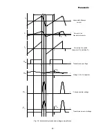
The peaking function is realized with
τ
= 160ns delay cells (i.e. frequency response reaches a
maximum at a frequency f = 1/2
τ
= 3.125MHz).
The coring function has a non-linear transfer characteristic which implies that a noise suppression
range (coring range) of 15 IRE is realized. This means that extra noise introduced due to increased
gain of the peaking amplifier is defeated by the coring function. The coring stage is activated via the
I²C bus (COR).
Asymmetric peaking is introduced to enhance picture definition. The negative/positive overshoot ratio
is approximately 1.8. The degree of peaking is controlled by the peaking amplifier via the I²C bus
(PEAKING). The output of the peaking amplifier is summed with the delayed (160ns) selected video
signal (see Fig 7).
The output of the peaking/coring stages (i.e. output of summing stage) is fed as internal luminance
signal (Y
INT
) to the YUV selection circuit (see YUV/RGB processing part).
SUMMING
STAGE
25IRE
100IRE
45IRE
Nominal PEAKING
PEAK
ASSYMETRIC
PEAKING
CORING
FUNCTION
COR
PEAKING
FUNCTION
15IRE
100IRE
(b1/wh)
Selected
VIDEO
Signal
DELAY
160ns
25IRE
45IRE
50IRE
50IRE
Fig 7: Peaking and coring operation


