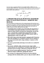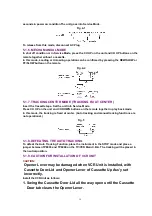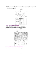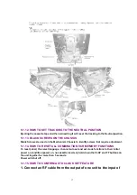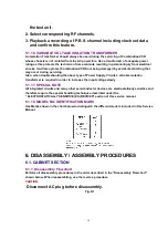
increased voltage is applied to IC5301 Pin11 through R514, R503 and R5504. Due to the
increased voltage at IC5301 Pin11, thehorizontal oscillator frequency increases, the picture goes
out of horizontal sync, the beam current decreases and the picture becomes dark in order to
keep X-radiation under specification.
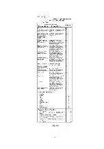
Figure 2
3. PREVENTION OF ELECTROSTATIC DISCHARGE
(ESD) TO ELECTROSTATICALLY SENSITIVE (ES)
DEVICES
Some semiconductor (solid state) devices can be damaged easily by static electricity. Such
components commonly are called Electrostatically Sensitive (ES) Devices. Examples of typical
ES devices are integrated circuits and some field-effect transistorsare semiconductor "chip"
components. The following techniques should be used to help reduce the incidence of
component damage caused by electrostatic discharge (ESD).
1. Immediately before handling any semiconductor component or
semiconductor-equipped assembly, drain off any ESD on your
body touching a known earth ground. Alternatively, obtain and
wear a commercially available discharging ESD wrist strap,
whichshould be removed for potential shock reasons prior to
applying power to the unit under test.
2. After removing an electrical assembly equipped with ES devices,
place the assembly on a conductive surface such as aluminum
foil, to prevent electrostatic charge buildup or exposure of the
assembly.
3. Use only a grounded-tip soldering iron to solder or unsolder ES
devices.
4. Use only an antistatic solder removal device. Some solder
removal devices not classified as "antistatic (ESD protected)" can
generate electrical charge sufficient to damage ES devices.
5. Do not use freon-propelled chemicals. These can generate
electrical charges sufficient to damage ES devices.
6. Do not remove a replacement ES device from its protective
package until immediately before you are ready to install it. (Most
7
Summary of Contents for OmniVision PV-C1324-K
Page 10: ...Fig 1 4 Fig 1 5 10 ...
Page 11: ...Fig 1 6 11 ...
Page 19: ...6 1 2 Disassembly Method Fig D2 19 ...
Page 20: ...Fig D3 20 ...
Page 21: ...6 1 2 1 Notes in chart 1 Removal of VCR Unit Fig D4 21 ...
Page 39: ...39 ...
Page 41: ...11 2 CHASSIS FRAME SECTION 1 41 ...
Page 42: ...11 3 CHASSIS FRAME SECTION 2 42 ...
Page 43: ...11 4 PACKING PARTS AND ACCESSORIES SECTION 43 ...
Page 60: ...R6079 ERJ6GEYJ102V MGF CHIP 1 10W 1K 60 ...
Page 65: ...C3035 ECJ2VC1H330J C CHIP 50V 33PF 65 ...
Page 74: ...13 2 CHASSIS FRAME SECTION 1 74 ...
Page 75: ...13 3 CHASSIS FRAME SECTION 2 75 ...
Page 76: ...13 4 PACKING PARTS AND ACCESSORIES SECTION 76 ...
Page 89: ...R554 ERDS2TJ123 CARBON 1 4W 12K 89 ...


