background image

81

KX-FT932BR-B

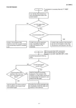
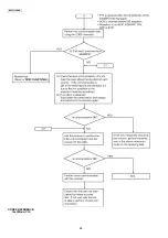
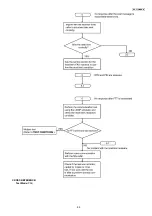
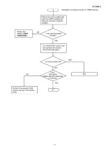
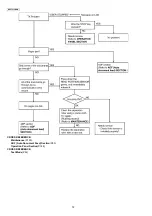
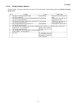
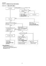
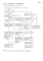
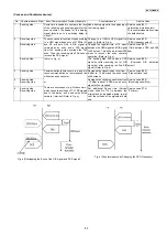
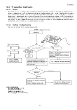
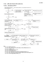
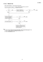
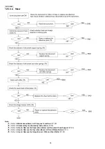
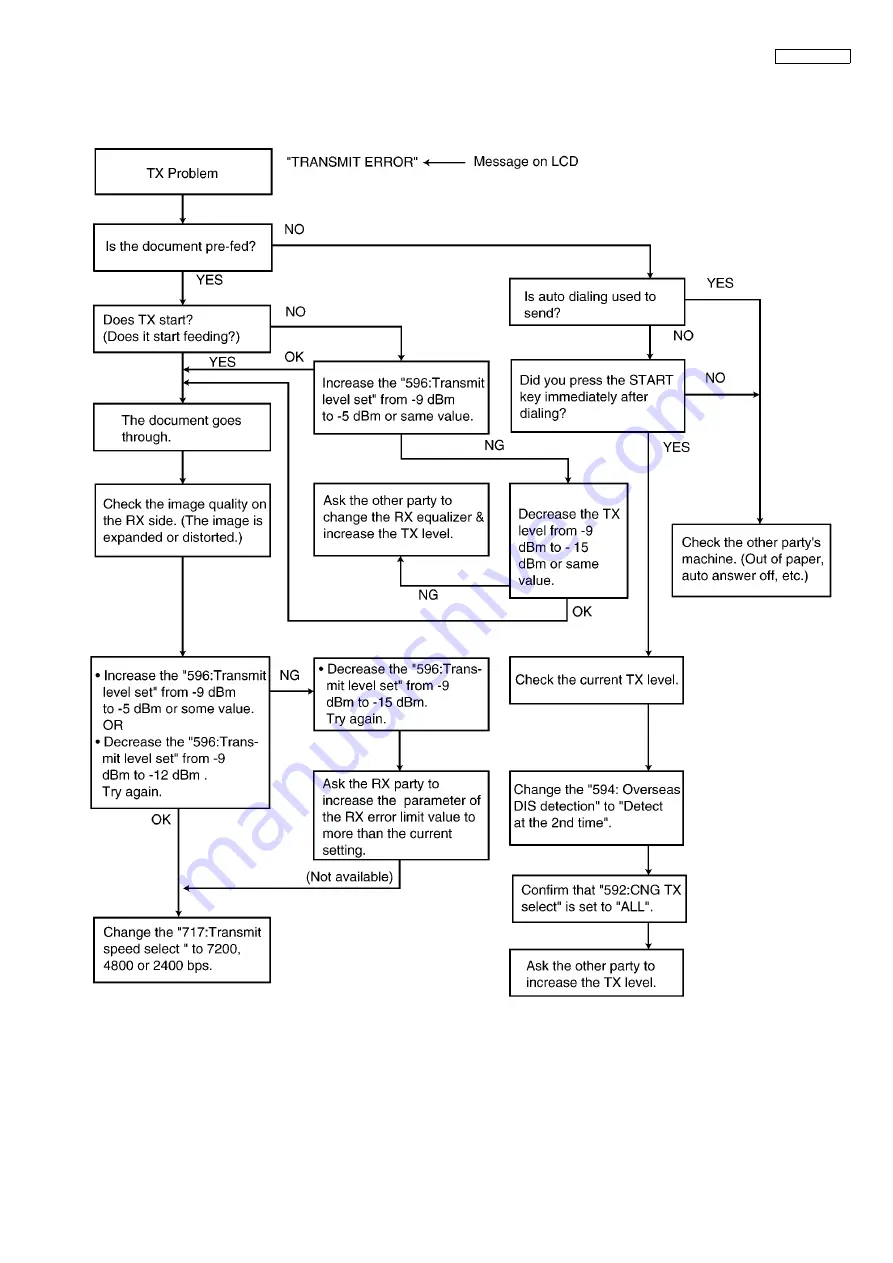
12.3.3.1.2. Sometime there is a transmit problem

Note:

Refer to 

Error Message (Display)

 (P.10) for display message.

Note:

• “596: Transmit level set” represents a service code. (Refer to 

Service Function Table

(P.57).)

Summary of Contents for KX-FT932BR-B

Page 1: ...07 Panasonic Communications Co Ltd All rights reserved Unauthorized copying and distribu tion is a violation of law Order No KMF0711129CE Personal Facsimile Model No KX FT932BR B B Black Version for Brazil ...

Page 2: ...55 10 3 Print Test Pattern 55 11 Service Mode 56 11 1 Programming and Lists 56 11 2 The Example of the Printed List 60 12 Troubleshooting Guide 64 12 1 Troubleshooting summary 64 12 2 Error Messages Display 65 12 3 Error Messages Report 66 12 4 Remote Programming 88 12 5 Troubleshooting Details 91 13 Service Fixture Tools 117 14 Disassembly and Assembly Instructions 118 14 1 Disassembly Flowchart ...

Page 3: ...lnerable to static electricity When repairing the following precautions will help prevent recurring malfunctions 1 Cover the plastic part s boxes with aluminum foil 2 Ground the soldering irons 3 Use a conductive mat on the worktable 4 Do not touch the IC or LSI pins with bare fingers 1 1 1 Suggested PBF Sloder There are several types of PbF solder available commercially While this product is manu...

Page 4: ...may be found on different areas of the same P C Board depending on manufacture date 1 2 AC Caution For safety before closing the lower cabinet please make sure of the following precautions 1 The earth lead is fixed with the screw 2 The AC lead is connected properly to power supply unit 3 Wrap the earth lead around the core 3 times 4 Wrap the AC lead around the core 2 times ...

Page 5: ... which are rotated by the document feed motor A gear rotates the two rollers Be careful not to touch them with your hands especially when the unit is operating 1 3 2 Live Electrical Sections All the electrical sections of the unit supplied with AC power by the AC power cord are live Never disassemble the unit for service with the AC power supply plugged in CAUTION AC voltage is supplied to the pri...

Page 6: ...es accumulate on a person For instance clothes rubbing together can damage electric elements or change their electrical characteristics In order to prevent static electricity touch a metallic part that is grounded to release the static electricity Never touch the electrical sections such as the power supply unit etc ...

Page 7: ...gher than its melting point approximately 1100 F 600 C When applying PbF solder to double layered boards please check the component side for excess which may flow onto the opposite side See figure below 2 2 Insulation Resistance Test 1 Unplug the power cord and short the two prongs of the plug with a jumper wire 2 Turn on the power switch 3 Measure the resistance value with an ohmmeter between the...

Page 8: ...ing Width 208 mm Transmission Time 1 Approx 15 s page Original mode 2 Scanning Density Horizontal 8 pels mm Vertical 3 85 lines mm in standard resolution 7 7 lines mm in fine photo resolution 15 4 lines mm in super fine resolution Photo resolution 64 level Scanner Type Contact Image Sensor Printer Type Thermal printing Data Compression System Modified Huffman MH Modified READ MR Modem Speed 9 600 ...

Page 9: ...cified recording paper Using other recording paper may affect print quality and or cause excessive wear to the thermal head 4 2 Translation Lists 4 2 1 Other 4 2 2 Error Message Report Model No Item Specifications Usage KX A106 Standard thermal recording paper 1 216 mm 30 m roll with 25 mm core ...

Page 10: ...ing function Phonebook function 100 names Caller ID compatible Feature requires a subscription to caller identification ser vices offered by certain local telephone companies for a tee You and your caller s must be in areas that provide caller identification services and compatible equipment must be used by both telephone companies Feature not available when the unit is connected to a PBX system E...

Page 11: ...11 KX FT932BR B 6 Technical Descriptions 6 1 Connection Diagram ...

Page 12: ... unit operations This memory is used mainly for the parameter working in the storage area 3 Dynamic RAM IC4 This memory is used mainly for the parameter working in the storage area 4 MODEM IC5 Performs the modulation and the demodulation for FAX communication 5 Read Section CIS image sensor to read transmitted documents 6 Motor Driver IC7 Drives the transmission motor and the reception motor 7 The...

Page 13: ...CPU OP PANEL I F 256kbit ROM 64Kbit SRAM A D IMAGE PROCESSING RTC SERIAL I F MOTOR I F PRINTER CONTROL VOL TONE 32 768KHz OSC 24MHz MOTOR SPEAKER HANDSET To FLASH PROGRAMMER 24 6V REG REG 5V 6V 24V 6V GATE ARRAY LCD PANEL English 2 lines Tact SW KEY MATRIX SENSOR x2 Doc sensor Read position sensor MESSAGE MIC FLASH 4Mbit TAM Model 3 3V IC6 LINERX CPC MONRX LINE Relay Transformer LINETX JAM HOOK PA...

Page 14: ... 3V POWER SOURCE ANALOG 3 3V 3 AIN1 A 3 3V CIS IMAGE SIGNAL INPUT ATN1 4 AIN2 A 3 3V THERMISTOR TEMPERATURE WATCH INPUT 5 AIN3 A 3 3V LINE VOLTAGE DETECTION SIGNAL INPUT DCIN 6 AMON A 3 3V ANALOG SIGNAL MONITOR TERMINAL 7 VSS GND POWER SOURCE GND 8 X32OUT O 3 3V BATT RTC 32 768KHz CONNECTION 9 X32IN I 3 3V BATT RTC 32 768KHz CONNECTION 10 VDD 3 3V B POWER SOURCE 3 3V LITHIUM BATTERY 11 XBACEN I 3 ...

Page 15: ...DATA BUS 4 69 DB1 I O 3 3V CPU DATA BUS 1 70 DB5 I O 3 3V CPU DATA BUS 5 71 VDD 3 3V POWER SOURCE 3 3V 72 VSS GND POWER SOURCE GND 73 VSS GND POWER SOURCE GND 74 VDD 3 3V POWER SOURCE 3 3V 75 DB0 I O 3 3V CPU DATA BUS 0 76 DB6 I O 3 3V CPU DATA BUS 6 77 DB7 I O 3 3V CPU DATA BUS 7 78 XROMCS O 3 3V FLASH IC2 CHIP SELECT 79 RD O 3 3V CPU RD 80 WR O 3 3V CPU WR 81 ADR0 O 3 3V CPU ADDRESS BUS 0 82 ADR...

Page 16: ...HASE 124 RXE IOP O 3 3V MOTOR ENABLE 125 TMO O 3 3V OUTPUT PORT NC 126 VDD 2 5V POWER SOURCE 2 5V 127 VSS GND POWER SOURCE GND 128 TM1 IOP O 3 3V OUTPUT PORT ACK_EN 129 TM2 IOP O 3 3V OUTPUT PORT CISON 130 TM3 IOP O 3 3V OUTPUT PORT RLY 131 TXE IOP I 3 3V INPUT PORT CUT_POS 132 KSTART O 3 3V OPERATION PANEL CONTROL 133 KLATCH O 3 3V OPERATION PANEL CONTROL 134 KSCLK O 3 3V OPERATION PANEL CONTROL ...

Page 17: ... F600H F7FFH DRAM access window 2 6 3 4 Reset Circuit Watch dog timer The output signal reset from pin 4 of the voltage detect IC IC3 is input to the ASIC IC1 114 pin 1 During a momentary power interruption a positive reset pulse of 50 70 msec is generated and the system is reset com pletely 2 The watch dog timer built in the ASIC IC1 is initialized by the CPU about every 1 5 ms When a watch dog e...

Page 18: ...power is turned ON power is supplied to RTC IC1 At this time the voltage at pin 14 of RTC IC1 is 3 3V When the power is turned OFF the battery supplies the power to RTC through J1 R80 D503 At that time the voltage at pin 14 of IC1 are about 2 5V When the power is OFF and the 5V and 3 3V voltages decrease the LOW is input to pin 114 of IC1 Pin 111 of IC1 outputs the reset signals Pin 11 of IC1 beco...

Page 19: ... A In point C according to the voltage output time the thermal head s temperature is detected After the thermal head temperature is converted to voltage in B it is then changed to digital data in the A D converter inside IC1 The CPU decides the strobe width of the thermal head according to this value Therefore this circuit can keep the ther mal head at an even temperature in order to stabilize the...

Page 20: ...n via routes 4 and 5 they are stored in RAM 4 The white black data stored as above via routes 6 and 8 is input to the P S converter The white black data converted to serial data in the P S converter is input to the Thermal Head via route 9 and is printed out on recording paper Note Fine Reads 3 85 lines mm Super Fine Reads 7 7 lines mm Photo Reads 15 4 lines mm Transmission 1 Same processing as Co...

Page 21: ...21 KX FT932BR B 6 4 2 Block Diagram ...

Page 22: ...d upon the shift of dot increment 1728 all the shift registers become filled with data and a latch pulse is emitted to each IC from IC1 pin 118 THLAT With this latch pulse all the contents of the shift registers are latched to the latch registers Thereafter through the addition of strobes from the IC1 pins 103 104 only black dot locations 1 among latched data activates the driver and the current p...

Page 23: ...23 KX FT932BR B ...

Page 24: ...nd the transistor Q14 turns on This applies voltage to the light source to light it The contact image sensor is driven by each of the FTG F1 signals output from IC1 and the original image illuminated by the light source undergoes photoelectric conversion to output an analogue image signal AIN The analogue image signal is input to the system ASIC on AIN1 pin 3 of IC1 and converted into 8 bit data b...

Page 25: ...sing driver IC7 to go ON The motor coil is energized sequentially in 2 phase increments or 1 2 phase increments which causes a 1 step rotation A 1 step rotation is 0 13mm of recording paper or document paper The timing chart is below Stepping Motor Phase Pattern When the motor is OFF gate array IC1 pin 124 becomes a low level and Q2 and Q1 also turns OFF Instead of 24V 5V is suplied through D501 s...

Page 26: ...uit Location Sensor Sensor or Switch Name Message Error DIGITAL CN5 Motor Position Sensor CALL SERVICE ANALOG SW1 Recording Paper Sensor CHECK COVER and OUT OF PAPER SW2 Hook SW SW3 JAM Sensor PAPER JAMED Operation Panel SW39 Document Top Sensor REMOVE DOCUMENT SW38 Document Set Sensor CHECK DOCUMENT ...

Page 27: ...is no recording paper the plate is separated from the switch lever and the switch turns off Pin 20 of IC1 becomes a high level When there is recording paper the plate pushes the switch lever and the switch turns ON Pin 20 of IC1 becomes a low level Analog Board Signal IC1 119 Pin Home position Low level Other High level Signal IC1 20 Pin Paper Low level No paper High level ...

Page 28: ...tection switch for determining whether the recording paper edge is in the correct position or not If the recording paper cannot be detected correctly at the JAM sensor position even when recording paper is present then JAM is dis played If the recording paper is at the sensor position then the switch turns on the IC1 21pin switches to a high level Analog Board SW Signal ON Hook OFF High level IC1 ...

Page 29: ... of IC1 5 pin Operation becomes a high level Operation Board 6 5 6 Document Set Sensor SW38 When a document is set the SW becomes ON and input signal of IC1 6 pin Operation becomes a low level When there is no document the SW becomes OFF and the input signal of IC1 6 pin Operation becomes a high level Operation Board Signal IC1 5 pin Out of the Read Position High level At the Read Position Low lev...

Page 30: ...al Telecommunications Union ITU investigates and make recommendations on international standards for facsimiles 2 Definition of Each Group Group I G1 Official A 4 size documents without using formats which reduce the band width of a signal are sent over telephone lines Deter mined in 1968 Transmission for about 6 minutes at a scanning line density of 3 85 lines mm Group II G2 Using reduction techn...

Page 31: ... is time at the start of transmission when the functions at the sending and receiving sides are confirmed the transmission mode is established and transmission and reception are synchronized Image transmission time This is the time required for the transmission of document contents image data In general this time is recorded in the catalog etc Hold time This is the time required after the document...

Page 32: ... signals added to them Data signals are added to DIS and DCS signals Signal DIS Digital Identification Signal Identification Signal Format 00000001 Function Notifies the capacity of the receiving unit The added data signals are as follows Signal DCS Digital Command Signal Identification Signal Format X1000001 Example Some models do not support the following items Bit No DIS DTC DCS 1 Transmitter T...

Page 33: ...mum recording length capability A4 297 mm Unlimited A4 297 mm and B4 364 mm Invalid Maximum recording length A4 297 mm Unlimited B4 364 mm Invalid 21 22 23 0 0 0 0 0 1 0 1 0 1 0 0 0 1 1 1 1 0 1 0 1 1 1 1 Minimum scan line time capability of the receiver 20 ms at 3 85 l mm T7 7 T3 85 40 ms at 3 85 l mm T7 7 T3 85 10 ms at 3 85 l mm T7 7 T3 85 5 ms at 3 85 l mm T7 7 T3 85 10 ms at 3 85 l mm T7 7 1 2...

Page 34: ...ng side opti mizes the automatic equalizer etc according to this signal TCF Training Check Sends 0 continuously for 1 5 seconds at the same speed as the training signal CFR Confirmation to Receive X0100001 Notifies the sending side that TCF has been properly received If TCF is not properly received FTT Failure To Train X0100010 is relayed to the sender The sender then reduces the transmission spee...

Page 35: ...35 KX FT932BR B b Redundancy Compression Process Coding Mode This unit uses one dimensional MH format ...

Page 36: ...e NCU section and enters pin 47 of the modem IC5 The signals that enter pin 47 of the modem IC5 are demodulated in the board to digital image signals then placed on the data bus In this case the image signals from the telephone line are transmitted serially Hence they are placed on the bus in 8 bit units Here the internal equalizer circuit reduces the image signals to a long distance receiving lev...

Page 37: ...o pin 23 of ASIC IC1 on the digital board TEL LINE PC1 1 2 4 CN1 11 CN2 11 IC1 23 Note inside the digital board 6 7 3 ON OFF Hook Circuit Normally ON HOOK condition LINE RELAY RLY1 is OFF While OFF HOOK RLY1 turns ON This LINE RELAY is con trolled by pin 130 of IC1 through the Q7 ON HOOK IC1 130 Low Level Q7 OFF RLY1 OFF OFF HOOK IC1 130 High Level Q7 ON RLY1 ON 6 7 4 Pulse Dial Circuit Make state...

Page 38: ...f 2 5 dB from pin 2 The transmission signal is input from CN1 pin 5 and output to the TEL line through C11 R16 IC2 6 7 and T1 Without a side tone circuit the transmission signal would return to the reception amplifier via C28 R27 and R26 Here the signal output from CN1 pin 5 passes through C28 R23 R22 C21 and R18 and enters the amplifier IC2 pin 3 This is used to cancel the return portion of the t...

Page 39: ...gnal which is modulated in an FSK Frequency Shift Keying format Data 0 is a 1200 Hz sine wave and data 1 a 2200 Hz sine wave There are two type of the message format which can be received i e the single data message format and multiple data mes sage format The multiple data format allows to transmit the name and data code information in addition to the time and telephone number data When there is ...

Page 40: ...y To use this feature you must sub scribe to a Caller ID service The data for the Caller ID from the telephone exchange is sent before the first ring signal The data from the telephone exchange is sent by DTMF signal 2 Circuit Operation The Caller ID signal from TEL LINE is processed with MODEM IC5 Refer to Sgnal Route P 108 for the route of Caller ID DTMF signal ...

Page 41: ... and received voices to and from the handset 2 Signal path Refer to Sgnal Route P 108 6 8 3 Monitor Circuit for Each Signals 1 Function This circuit monitors various tones such as 1 DTMF tone 2 Alarm Beep Key tone Bell 3 Dummy ring back tone 2 Signal path Refer to Sgnal Route P 108 6 9 ATAS Automatic Telephone Answering System Section 6 9 1 Remote Receiving 1 Function This is the parallel connecti...

Page 42: ...45 R221 C38 C216 C29 R38 R35 PC1 13 CN2 CN1 L1 13 Analog Board Digital Board To IC5 5VA 1 2 3 4 D8 5V Q7 RLY1 1 2 RLY 24VA 2 0V R13 R11 R10 C8 C7 C17 R18 R2 2 R23 R2 6 R27 R1 4 R15 D1 C21 4 3 2 1 8 IC2 Ref R41 L19 C14 C28 C4 BELL R2 R54 R219 D506 R220 C217 R105 CN4 1 2 EXT TEL L26 L25 ...

Page 43: ...odes They are controlled by the Gate Array IC1 and ASIC IC1 on the DIGITAL BOARD The key matrix table is shown below CN1 CN206 IC1 ASIC Chip on board type LCD GATE ARRAY IC1 CN2 READ POSITION SENSOR DOCUMENT SENSOR 37 KEYS MATRIX LED DIGITAL BOARD OPERATION BOARD KX FT932BR B OPERATION BOARD BLOCK DIAGRAM XLED8 9 KIN0 7 XLED13 ...

Page 44: ...rive R25 R24 R15 and R17 are density control resistors Consequently in this unit the timing positive clock is generated by the LCD interface circuitry in the gate array IC1 DIsplay mode Density Normal Dark English font Global 2 lines LED1 IC1 22pin H L LED15 IC1 21pin L L LED14 IC1 20pin Hi Z L Chinese font 2 lines LED1 L H LED15 Hi Z H LED14 Hi Z H ...

Page 45: ... and D13 and charges C5 to make DC voltage Then it supplies power to the con verter circuit Kick on voltage circuit Bias is applied to the Q1 gate via this circuit when the AC power is turned on and Q1 begins operating Input Circuit AC Input Surge absorber circuit G H 9 6V 24V Kick on Voltage Circuit E F GND Control Circuit R2 R3 Converter Circuit C D 6V Output Circuit 24V Output Circuit Rectifier...

Page 46: ...ansfer as follows L D1 Load L Then the power is supplied to the Load When Q1 is ON power is not output from the secondary side The output voltage is fed back in the control circuit according to the error amp rectifier Then depending on how f is controlled stabilization occurs Also when the current load becomes too large in order to decrease the voltage output the increase in f is controlled and th...

Page 47: ...ws When the output voltage of the 24V circuit increases the current of the photo coupler PC101 increases the pulse width of the out put control circuit becomes higher and the ON period of Q101 becomes shorter Over Current Limiter O C L The highest drain current Q1 is limited by controlling f of Q1 of 24V The 24V output is limited by this circuit Over Voltage Circuit If the 24V output increases bec...

Page 48: ...48 KX FT932BR B 7 Location of Controls and Components 7 1 Overview 1 Speaker 2 Document guides 3 Document feeder tray 4 Top cover 5 Document exit 6 Document entrance 7 Top cover release button ...

Page 49: ...setting ON OFF 6 Station keys To use one touch dial feature 7 FAX START To start sending or receiving a fax 8 COPY To copy a document 9 TONE To change from pulse to tone temporarily during dialling when your line has rotary pulse services 10 PAUSE To insert a pause during dialing 11 MONITOR To initiate dialing without lifting the handset 12 BROADCAST To transmit a document to multiple parties 13 N...

Page 50: ...nt the unit from functioning properly To protect the unit from damage hold both sides when you move it 8 2 Connections Important The unit will not function when there is a power failure To make calls in emergency situations you should con nect a telephone that can function during a power fail ure to the telephone line 1 Power cord Connect to the power outlet 127V 60 Hz 2 Telephone line cord Connec...

Page 51: ... the top cover securely by pushing down on both sides 6 Press FAX START then tear off the excess paper by pulling it towards you Note If the paper is secured with glue or tape cut approxi mately 15 cm from the beginning of the roll before install ing it When the power cord is connected a message is printed each time the top cover is opened then closed If the recording paper is installed upside dow...

Page 52: ...other side such as newsprint Check that ink paste or correction fluid has dried com pletely To send a document with a width of less than 210 mm we recommend using a copy machine to copy the original docu ment onto A4 or letter sized paper then sending the copied document 9 Operating Instructions 9 1 Setting Your Logo Your logo will be printed on the top of each page sent from your unit The logo ca...

Page 53: ...ers alternately 1 Press 2 2 times 2 Press 4 3 times 3 Press 4 Press 5 3 times To correct a mistake 1 Press or to move the cursor to the incorrect character 2 Press STOP To erase all characters press and hold STOP 3 Enter the correct character To select characters using or Instead of pressing the dial keys you can select characters using or 1 Press repeatedly to display the desired character Charac...

Page 54: ...aper reverse Press STOP button to quit SET LED CHECK Service Mode 5 5 7 All LEDs above the operation panel board flash on and off or are illuminated SET LCD CHECK Service Mode 5 5 8 Checks the LCD indication Illuminates all the dots to check if they are normal Refer to Operation Panel Section P 113 SET KEY CHECK Service Mode 5 6 1 Checks the button operation Indicates the button code on the LCD wh...

Page 55: ...0 3 Print Test Pattern key High Frequency Hz key Low Frequency Hz 1 697 5 1209 2 770 6 1336 3 852 7 1477 4 941 8 1633 High Hz 1209 1336 1477 Low Hz 697 1 2 3 770 4 5 6 852 7 8 9 941 0 Code Button Name Code Button Name Code Button Name 04 FAX START 31 1 3D PAUSE 05 LOWER 32 2 3E FLASH RECALL 06 COPY 33 3 47 CALLER ID 08 MONITOR 34 4 64 STATION 1 0C AUTO ANSWER 35 5 65 STATION 2 0F REDIAL 36 6 66 ST...

Page 56: ...se listed in the Operating Instructions and are available to the user The special programs are only those listed here and not displayed to the user In both the User and Ser vice Modes there are Set Functions and Test Functions The Set Functions are used to program various features and functions and the Test Functions are used to test the various functions The Set Functions are accessed by entering...

Page 57: ...heck See Test Mode P 54 556 Motor test 00 See Test Mode P 54 557 LED test See Test Mode P 54 558 LCD test See Test Mode P 54 559 Document jam detection select 1 ON 2 OFF 1 2 1 See Test Mode P 54 561 KEY test See Test Mode P 54 570 BREAK select 1 61 2 67 1 2 2 Sets the break of pulse dialing according PBX 571 ITS auto redial time set X number of times 00 99 05 Selects the number of times that ITS i...

Page 58: ... Receive Problem P 82 and The unit can copy but the transmission and reception image are incorrect P 86 722 Redial tone detect 1 ON 2 OFF 1 2 1 Sets the tone detection mode after redialing 731 CPC mode 1 A 2 B 3 OFF 1 2 3 3 Set the CPC signal detection mode from the converter 745 Power ON film feed 1 ON 2 OFF 1 2 1 Invalid function for thermal model 763 CNG detect time for friendly reception 1 10 ...

Page 59: ... 1 Execute Service Mode 550 when you want to reset the all setting data keeping the user information 2 Execute Service Mode 710 to clear the user information in case that Main Unit is recycled Note Please restart a power supply after clearing a memory ...

Page 60: ...60 KX FT932BR B 11 2 The Example of the Printed List 11 2 1 User Mode Example of a printed out list ...

Page 61: ...61 KX FT932BR B 11 2 2 Service Mode Example of a printed out list ...

Page 62: ... KX FT932BR B 11 2 3 History Example of a printed out list Note See the following descriptions of this report Item No 1 44 are corresponding to the listed items in Descriptions of the History Report P 63 ...

Page 63: ... The amount of time the TEL FAX mode setting was used 16 Not used 17 FINAL RECEIVE MODE The last set receiving mode by the user 18 TONE PULSE SELECTION The most recently used setting used either TONE or PULSE 19 RECEIVE REDUCTION The compression rate when receiving 20 SETTING NO OF DIRECTORY The recorded directory stations 21 NUMBER OF COPY The number of pages copied 22 NUMBER OF RECEIVE The numbe...

Page 64: ...lection lever paper thickness lever is set correctly and the paper is set correctly without any slack 2 Before troubleshooting first check that the connectors and cables are connected correctly not loose If the problem occurs randomly check it very carefully 3 When connecting the AC power cord with the unit and checking the operation exercise utmost care when handling electric parts in order to av...

Page 65: ...x memory capacity Refer to Specifications P 8 The memory is full of received documents due to lack of recording paper or a recording paper jam Install paper or clear the jammed paper Refer to Jams P 137 When performing broadcast transmission the document being stored exceeded the memory capacity of the unit Send the entire document manually There is no space to store new items in the phonebook Era...

Page 66: ...e after post message is transmitted three times 4 44 COMMUNICATION ERROR SND RTN and PIN are received 5 46 COMMUNICATION ERROR RCV No response after FTT is transmitted 6 48 COMMUNICATION ERROR RCV No post message 7 49 COMMUNICATION ERROR RCV RTN is transmitted 8 50 COMMUNICATION ERROR RCV PIN is transmitted to PRI Q 8 51 COMMUNICATION ERROR RCV PIN is transmitted 8 OTHER FAX NOT RESPONDING RCV Rec...

Page 67: ...67 KX FT932BR B ...

Page 68: ...68 KX FT932BR B CROSS REFERENCE Test Mode P 54 ...

Page 69: ...69 KX FT932BR B CROSS REFERENCE Test Mode P 54 ...

Page 70: ...70 KX FT932BR B CROSS REFERENCE Test Mode P 54 ...

Page 71: ...71 KX FT932BR B ...

Page 72: ...72 KX FT932BR B CROSS REFERENCE Maintenance P 129 ADF Auto Document Feed Section P 93 Operation Panel Section P 168 CROSS REFERENCE Test Mode P 54 ...

Page 73: ...73 KX FT932BR B ...

Page 74: ...74 KX FT932BR B ...

Page 75: ...75 KX FT932BR B CROSS REFERENCE Test Mode P 54 ...

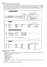
Page 76: ... you basic information about a communication but the other two journal reports provide different informa tion on the same item communication HOW TO READ JOURNAL REPORTS Example 1 Look at NO 01 in the JOURNAL If you want to know about the details about that item see NO 01 in the JOURNAL 2 and the JOURNAL 3 You can get the following information MODE Fax transmission RCV MODE TEL TX SPEED 9 6 kbps RE...

Page 77: ...emory due to PAPER OUT error NO RESPONSE DISAPPEARED ON JOURNAL The NO RESPONSE DISAPPEARED ON JOURNAL displays the information about the last 10 communications terminated by No Response Some of the communications terminated by No Response were not displayed in the JOURNAL When a fax transmission cannot be performed because the other party s unit is set to the TEL mode No response will be printed ...

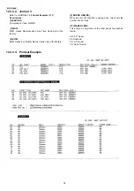
Page 78: ...Scan Line Time Used only at the factory 8 EQM EQM means Eye Quality Monitor Used only at the factory 9 ERROR LINE RX When an error occurs while receiving a fax this shows the number of error lines 10 MAKER CODE This shows a 2 digit code of the other party s fax machine brand 0E KX model 00 Unknown 79 UF model 19 Xerox model 12 3 2 3 Printout Example ...

Page 79: ...essfully but sometimes fails The unit can copy documents Troubleshooting Problem with the service line or with the transmitter s fax 4 The fax completely fails to transmit or receive The unit can copy documents Troubleshooting Problem with the electric circuit 5 The fax fails either to transmit or receive when making a long distance or an international call The unit can copy documents Detailed des...

Page 80: ...80 KX FT932BR B 12 3 3 1 Defective Facsimile Section 12 3 3 1 1 Transmit Problem CROSS REFERENCE Operation Panel Section P 113 ADF Auto Document Feed Section P 93 Maintenance P 129 ...

Page 81: ...T932BR B 12 3 3 1 2 Sometime there is a transmit problem Note Refer to Error Message Display P 10 for display message Note 596 Transmit level set represents a service code Refer to Service Function Table P 57 ...

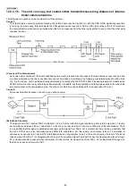
Page 82: ...ated problems such as OUT OF PAPER when the fax switches to the memory receiving mode and the memory capacity becomes full of the unprintable data In this case error mes sages MEMORY FULL and its main cause for example CHECK PAPER are displayed on the LCD Once you solve the main problem MEMORY FULL will be cancelled and the reception problem will be resolved LCD display messages indicating the err...

Page 83: ...83 KX FT932BR B 12 3 3 1 4 The unit can copy but cannot transmit receive CROSS REFERENCE Analog Board Section P 108 Test Mode P 54 ...

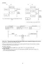
Page 84: ...should be called manually if possible Another possibility is entering two pauses at the end of the auto dial number on the transmission side Then the count start time can be delayed for 2 pauses about 10 sec Cause 2 Erroneous detection because of an echo or an echo canceler Echo Echo Canceler The signal from FAX1 reaches FAX2 via stations 1 and 2 but the reflection signal at station 2 also returns...

Page 85: ...ge the regular rime of 75 msec between the CED signal and DIS signal to 500 msec This will give at least 250 msec to recover the echo canceler operation Refer to Fig c Service code 593 Time between CED and 300 bps Sending side The sending side FAX sends a DCS signal not after receiving the 1st DIS signal but after receiving the 2nd DIS signal Refer to Fig d Service code 594 Overseas DIS detection ...

Page 86: ...e other FAX unit and the line conditions The countermeasures for this unit are shown below Transmission Operation Set the transmitting speed to 4800BPS service mode code No 717 or select the overseas mode Reception Operation If 80 or more of the reception is incorrect set the receiving speed to 4800BPS Service mode code No 718 Refer to Service Function Table P 57 TX side signal RX side signal Coun...

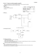
Page 87: ...control setting Refer to the PC instruction book 2 Start up the PC software SOUND RECORDER This software is bundled to Windows OS which can create WAV file Set the audio format PCM 22 050kHz 8bit mono 3 Click the record button and start recording after acquisition the signal Note Not to be wind wave patterns on the wave monitor Please compress the recording data when you send attaching to E Mail b...

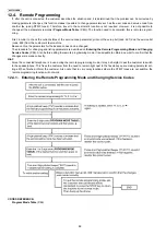
Page 88: ...omer s fax machine Based on this the parameters for the desired codes can be changed The procedure for changing and listing parameters is described on Entering the Remote Programming Mode and Changing Service Codes P 88 Also before exiting the remote programming mode it is advisable to obtain a new list to confirm that the changes were made correctly Hint Since the connected telephone is in use du...

Page 89: ...1 ON 2 OFF ON OK 523 Receive equalizer select 1 0km 2 1 8km 3 3 6km 4 7 2km 0km OK 524 Transmission equalizer select 1 0km 2 1 8km 3 3 6km 4 7 2km 0km OK 544 Document feed position adjustment value set 1 3mm 2 4mm 3 5mm 4 6mm 5 7mm 5mm OK 550 Memory clear NG 551 ROM check NG 552 DTMF signal tone test 1 ON 2 OFF OFF OK 553 Monitor on FAX communication 1 OFF 2 Phase B 3 ALL OFF OK 554 Modem test NG ...

Page 90: ... Print test pattern NG 853 Top margin 1 9 mm 3 OK 874 DTMF ON time 06 20msec 10ms OK 875 DTMF OFF time 06 20msec 10ms OK 880 History list 1 SET NG 881 Journal 2 1 SET NG 882 Journal 3 1 SET NG 961 The time transmitting the false ring back tone 01 10 x sec 05sec OK 962 The operator calling time 05 30 x sec 13sec OK 991 Setup list 1 Start OK 994 Journal list 1 Start OK 995 Journal 2 list 1 Start OK ...

Page 91: ...y use different expressions for the same problem as they are not a technician or engineer Using your experience test the problem area corresponding to the claim Also returns from a customer or dealer often have a claim tag For these cases as well you need to determine the problem Test the unit using the simple check list on Simple Check List P 92 Difficult problems may be hard to determine so repe...

Page 92: ...ng an Abnormal Sound is Heard from the Unit P 99 Power supply Voltage output is abnormal See Power Supply Board Section P 110 Operation panel Keys are not accepted See Operation Panel Section P 113 Sensor If the electric circuit is the cause the error mes sage corresponding to the sensor will be dis played See Sensor Section P 114 SERIAL NO DATE FUNCTION JUDGEMENT REFERENCE FAX operation Transmiss...

Page 93: ...ve the Operation Board LCD and Platen Roller P 121 3 Refer to Test Mode P 54 4 Refer to Digital Board Section P 100 5 Refer to Sensor Section P 114 6 Refer to How to Remove the Gear Block and Separation Roller P 127 7 Refer to How to Remove the Separation Holder and Document Feed Support P 122 8 Refer to Power Supply Board Section P 110 ...

Page 94: ...2BR B 12 5 4 2 Document Jam CROSS REFERENCE Test Mode P 54 Sensor Section P 114 Note 1 Refer to How to Remove the Operation Board LCD and Platen Roller P 121 2 Refer to Disassembly and Assembly Instructions P 118 ...

Page 95: ... KX FT932BR B 12 5 4 3 Multiple Feed Note 1 Refer to How to Remove the Separation Holder and Document Feed Support P 122 2 Refer to Disassembly and Assembly Instructions P 118 3 Refer to Maintenance P 129 ...

Page 96: ...ons P 129 2 Refer to Disassembly and Assembly Instructions P 118 3 Refer to How to Remove the Separation Holder and Document Feed Support P 122 4 Refer to How to Remove the Operation Board LCD and Platen Roller P 121 5 Refer to How to Remove the Image Sensor CIS and Feed Roller P 123 ...

Page 97: ...E Thermal Head Section P 116 Test Mode P 54 CIS Contact Image Sensor Section P 115 Note 1 Refer to Maintenance Items and Componet Locations P 129 2 Refer to Disassembly and Assembly Instructions P 118 3 Refer to How to Remove the Operation Board LCD and Platen Roller P 121 ...

Page 98: ...o How to Remove the Lock Lever and Thermal Head P 124 2 Refer to Maintenance Items and Componet Locations P 129 3 Refer to How to Remove the Operation Board LCD and Platen Roller P 121 4 Refer to How to Remove the Image Sensor CIS and Feed Roller P 123 12 5 4 7 Skewed Receiving Image Note 1 Refer to Installing the Recording Paper P 51 ...

Page 99: ...from the Unit Note 1 Refer to Document Feeder Cleaning P 138 2 Refer to Thermal Head Cleaning P 138 3 Refer to Disassembly and Assembly Instructions P 118 4 Refer to How to Remove the Motor of Gear Block P 127 5 Refer to How to Remove the Gear Block and Separation Roller P 127 ...

Page 100: ...LASH ROM malfunctions are extremely rare after installation in the product This may be repaired by replacing the IC DRAM etc However the real cause may not have been an IC malfunction but a sol dering fault instead Soldering faults difficult to detect with the naked eye are common particularly for ASIC and RA Resistor Array But if you have an oscilloscope you can easily determine the problem site ...

Page 101: ...LCD Key And serial interface UART connects both systems Flash memory IC2 in the ASIC system is for software and also for user memory settings Phone book CID memory DRAM IC4 in the ASIC system is for work memory and also for fax memory The signal lines that must be normal for the system to boot up are listed here List 1 For signal lines other than these even if they malfunction they do not directly...

Page 102: ...102 KX FT932BR B NG Wave pattern Note Refer to NG Example P 107 ...

Page 103: ...of these signals If the timing of these signals is even slightly delayed the circuit will not work Nor will it if the IC is defective and the output voltage level is not normal although the timing of these signals is accurate enough to meet the specifications Make sure that your oscilloscope is calibrated before starting a test Therefore it is imperative to confirm whether each IC outputs the sign...

Page 104: ...104 KX FT932BR B I O and Pin No Diagram ...

Page 105: ...105 KX FT932BR B 12 5 5 2 Check the Status of the Digital Board First please check voltages and oscillation whether they are correct as follows ...

Page 106: ...106 KX FT932BR B ...

Page 107: ...107 KX FT932BR B 12 5 5 3 NG Example ...

Page 108: ...handset microphone and the signal is output to the telephone line The signal mainly flowing on this route is analog You can trace the signal with an oscilloscope The signal flow on each route is shown in the Check Sheet here If you find a specific problem in the unit for example if you cannot communicate with the MONITOR trace that signal route locally with the following Check Sheet and locate the...

Page 109: ...ion reception Following the ITS section or NCU section search for the route between the microphone and the telephone line sending or between the telephone line and the speaker receiving where the signal disappears Check the components at that point 2 No pulse dialing 3 No ring tone or No bell 4 No tone dialing ...

Page 110: ...ltage test withstanding voltage test intentional short circuit test etc Caution If you find a melted fuse in the unit do not turn on the power until you locate and repair the faulty parts except for the fuse otherwise the fuse will melt again and you cannot pinpoint the faulty point In most cases the symptom is that nothing is output It is more likely that the fault is in the primary side rather t...

Page 111: ...111 KX FT932BR B 12 5 7 2 Troubleshooting Flow Chart ...

Page 112: ...1 Q1 The worst case of Q1 is a short circuit between the Drain and Gate because damage expands to the peripheral circuit of Q1 This is due to a very high voltage through the Gate circuit which is composed of R19 Q2 and Q21 etc You should change all of the parts listed as follows F1 Q1 R19 Q2 Q21 D101 D104 If D101 and D104 are broken the oscillation circuit in the power supply cannot operate Check ...

Page 113: ...113 KX FT932BR B 12 5 8 Operation Panel Section 12 5 8 1 No Key Operation CROSS REFERENCE Test Mode P 54 12 5 8 2 No LCD Indication CROSS REFERENCE Test Mode P 54 ...

Page 114: ...P 26 for the circuit descriptions 12 5 9 1 Check the Document Sensor SW39 CHECK DOCUMENT Note Refer to Error Message Display P 10 for display message 12 5 9 2 Check the Read Position Sensor SW38 REMOVE DOCUMENT Note Refer to Error Message Display P 10 for display message ...

Page 115: ...115 KX FT932BR B 12 5 10 CIS Contact Image Sensor Section Refer to Scanning Block P 24 CROSS REFERENCE Test Mode P 54 ...

Page 116: ...116 KX FT932BR B 12 5 11 Thermal Head Section Refer to Thermal Head P 22 ...

Page 117: ...117 KX FT932BR B 13 Service Fixture Tools ...

Page 118: ... Block P 120 A 2 How to Remove the Operation Board LCD and Platen Roller P 121 A 3 How to Remove the Separation Holder and Document Feed Support P 122 A 4 How to Remove the Image Sensor CIS and Feed Roller P 123 A 5 How to Remove the Lock Lever and Thermal Head P 124 B 1 How to Remove the Bottom Frame P 125 B 3 How to Remove the Gear Block and Separation Roller P 127 ...

Page 119: ...SS REFERENCE B 1 How to Remove the Bottom Frame P 125 B 2 How to Remove the Analog Board Digital Board Power Supply Board and Power Cord P 126 B 3 How to Remove the Gear Block and Separation Roller P 127 B 4 How to Remove the Motor of Gear Block P 127 ...

Page 120: ...120 KX FT932BR B 14 2 Disassembly Procedurel 14 2 1 How to Remove the Operation Panel Block ...

Page 121: ...121 KX FT932BR B 14 2 2 How to Remove the Operation Board LCD and Platen Roller ...

Page 122: ...122 KX FT932BR B 14 2 3 How to Remove the Separation Holder and Document Feed Support ...

Page 123: ...123 KX FT932BR B 14 2 4 How to Remove the Image Sensor CIS and Feed Roller ...

Page 124: ...124 KX FT932BR B 14 2 5 How to Remove the Lock Lever and Thermal Head ...

Page 125: ...125 KX FT932BR B 14 2 6 How to Remove the Bottom Frame ...

Page 126: ...126 KX FT932BR B 14 2 7 How to Remove the Analog Board Digital Board Power Supply Board and Power Cord ...

Page 127: ...127 KX FT932BR B 14 2 8 How to Remove the Gear Block and Separation Roller 14 2 9 How to Remove the Motor of Gear Block ...

Page 128: ...128 KX FT932BR B 14 2 10 Installation Position of the Lead Wires ...

Page 129: ...and communication testing to determine if the problem originates from the transmitter receiver or the telephone line 4 Determine causes Determine the causes of the equipment problem by troubleshooting 5 Equipment repairs Repair or replace the defective parts and take appropriate measures at this stage to ensure that the problem will not recur 6 Confirm normal operation of the equipment After compl...

Page 130: ...124 5 Sensors Document sensor SW39 Read position sensor SW38 Record ing paper cover open sensor SW1 Jam sensor SW3 Hook switch SW2 Confirm the operation of the sensors See Maintenance check Items Componet Locations P 129 6 Glass If the glass is dirty clean them with a dry soft cloth Refer to Document Feeder Cleaning P 138 7 Abnormal wear and tear or loose parts Replace the part Check if the screws...

Page 131: ... 2 1 Mode Selection When the motor attached to the Drive Motor Gear rotates counterclockwise CCW Swing Gear A engages the CAM and the CAM turns counterclockwise to select a mode See Fig A There are three mode options controlled by the Switch A Transmit mode B Receive mode and C Copy mode In Fig B you can see which mode is selected by the position of the rib in the CAM Fig A ...

Page 132: ...Gear A 1 controls the mode opera tion 15 2 2 1 TX Mode Swing Gear A engages Gear TX and conveys its drive power to the Separation Roller Gear for pre feeding documents Fig B TX mode 15 2 2 2 RX Mode Swing Gear B engages Gear RX and conveys its drive power to the Platen Roller Gear for printing the received data Fig C RX mode ...

Page 133: ...Separation Roller Gear and the Platen Roller Gear for feeding documents and recording paper in the copying operation Fig D Copy mode 15 2 2 4 Reverse Mode Swing gear D engages between swing gear B and gear RX and conveys its drive power to the platen roller gear for reversing the recording paper Fig E Reverse mode ...

Page 134: ...134 KX FT932BR B 15 2 3 Mechanical Movements in the Main Operations 15 2 3 1 Idle Status ...

Page 135: ...135 KX FT932BR B 15 2 3 2 Scanning CROSS REFERENCE Sensor Section P 114 Error Messages Display P 65 15 2 3 3 Printing Note See Sensors and Switches P 26 ...

Page 136: ...136 KX FT932BR B 15 2 3 4 Copying CROSS REFERENCE Sensor Section P 114 ...

Page 137: ...e recording paper and close the top cover securely by pushing down on both sides See page Installing the Recording Paper P 51 15 3 2 Document Jams Sending 1 Open the top cover by pressing the top cover release but ton and remove the jammed document carefully 2 Close the top cover securely by pushing down on both sides Note Do not pull out the jammed paper forcibly before opening top cover ...

Page 138: ... the power cord and the telephone line cord 5 Close the top cover securely by pushing down on both sides 15 4 2 Thermal Head Cleaning If smudges or black white lines appear on a copied received document check whether there is dust on the thermal head Clean it to remove the dust 1 Disconnect the power cord and the telephone line cord 2 Open the top cover by pressing the top cover release but ton an...

Page 139: ...139 KX FT932BR B 16 Miscellaneous 16 1 Terminal Guide of ICs Transistors and Diodes 16 1 1 Digital Board 16 1 2 Analog Board 16 1 3 Operation Board ...

Page 140: ...140 KX FT932BR B 16 1 4 Power Supply Board ...

Page 141: ... Flux Recommended Flux Specific Gravity 0 82 Type RMA lower residue non cleaning type Note See About Lead Free Solder PbF Pb free P 7 16 2 2 Flat Package IC Removal Procedure 1 Put plenty of solder on the IC pins so that the pins can be completely covered Note If the IC pins are not soldered enough you may give pressure to the P C board when cutting the pins with a cutter 2 Make a few cuts into th...

Page 142: ...of the IC setting with the corresponding soldering foil 2 Apply flux to all pins of the FLAT PACKAGE IC 3 Solder the pins sliding the soldering iron in the direction of the arrow 16 2 4 Bridge Modification Procedure 1 Lightly resolder the bridged portion 2 Remove the remaining solder along the pins using a soldering iron as shown in the figure below ...

Page 143: ...143 KX FT932BR B 16 3 Test Chart 16 3 1 ITU T No 1 Test Chart ...

Page 144: ...144 KX FT932BR B 16 3 2 ITU T No 2 Test Chart ...

Page 145: ...145 KX FT932BR B MEMO ...

Page 146: ...TART 133 KLATCH 134 KSCLK 135 KTXD 136 KRXD 137 FMEMCLK IOP24 138 FMEMDI IOP25 139 ADSEL1 140 VDDA2 5V 141 VREFB 142 VCL 143 VREFT 144 VSSA D505 BR6 10V D502 BR1 10V 1 A11 2 A9 3 A8 4 A13 5 A14 6 A17 7 WE 8 VDD 9 A18 10 A16 11 A15 12 A12 13 A7 14 A6 15 A5 16 A4 17 A3 18 A2 19 A1 20 A0 21 D0 22 D1 23 D2 24 VSS 25 D3 26 D4 27 D5 28 D6 29 D7 30 CE 31 A10 32 OE 1 VDD 2 GND 3 VOUT 4 VDET 5 CE 1 INB 2 I...

Page 147: ... 4 7K R36 4 7K R38 24K R130 R129 NC 330K R127 36K R128 39K R126 R125 NC 3 3K R131 47K R124 R121 NC R120 NC R119 NC R118 NC R117 NC R115 NC R114 NC R116 NC R113 NC L11 NC L10 NC L12 NC L9 NC Q17 NC Q18 NC R225 NC 20K R226 R217 NC R216 NC R214 2 7K R232 4 7K 0 R200 0 R231 47K R228 L4 NC L3 NC 1K R229 15K R140 10K R142 R96 10 3 3K R90 R93 2 2K R94 22K 1 5K R95 Q13 12K R75 8 2K R76 1K R164 R163 150 R1...

Page 148: ... 11 BELL DCN 12 HOOK 13 LINERX 14 MONRX 15 H STX_MUTE 16 H SRX C6 6 3V47u C10 6 3V47u 5VA 1 2 3 4 8 5 6 7 22 R100 AG L34 1 Q2 Q3 Q4 NC Q5 NC T1 1 2 3 4 6 0 R47 Q13 NC R87 NC AG 100 R1 D1 1 4 7V K0 033u C63 C26 NC C35 NC C66 NC C3 NC C27 NC C78 NC K0 1u C12 K0 1u C30 K0 022u C25 C29 K0 01u D10p C22 C13 D10p J22p C23 C20 Z0 1u Z0 1u C31 C7 Z0 1u C72 Z0 1u C18 NC C19 K0 015u C24 Z0 1u 150 2W R41 R27 ...

Page 149: ...1 b1 2 a1 R62 NC C47 6 3V47u D8 C42 NC L21 L23 L24 L22 D10 NC 1 2 3 4 Q12 NC R83 NC AG 5VA 22 R52 L31 L32 L25 Q7 R102 NC AG R104 NC AG Q8 PC4 NC AK KA E C C43 NC PC2 NC AK KA E C AG C80 NC RLY1 1 3 5 4 5V RLY1 2 1 2 D4 0 D5 0 250V 1uF C38 D13 NC C68 NC R86 NC D15 NC C67 NC R88 NC R84 NC R85 NC PC6 NC A K E C 5VA DA3 1 2 3 SA2 1000V C37 NC C44 NC C79 NC R54 0 R38 15K 1 2W K0 1u C51 C33 K0 1u C46 K0...

Page 150: ...W14 3 SW15 6 SW16 SW17 MONITOR SW18 SW19 FLASH PAUSE SW20 REDIAL SW21 NAVI LEFT SW22 NAVI DOWN SW23 NAVI UP SW24 NAVI RIGHT SW25 NAVI CENTER SW26 BOARDCAST SW27 SKEY 3 SW28 SKEY 2 SW29 RECORD NC SW30 SKEY 1 SW31 SKEY 6 SW32 MENU SW33 AUTO ANSWER SW34 SKEY 5 SW35 SKEY 4 SW36 ERASE NC SW37 PLAYBACK NC MIC MIC C14 J120p 0 R14 C13 K330p SW38 1 2 3 4 4 7K R23 100 R21 K0 01u C20 5V CN2 1 VSS 2 VDD 3 V0 ...

Page 151: ...2 R23 D20 D9 R9 R12 R13 R11 D4 D105 C102 D107 D110 C112 R113 R413 R412 R411 C411 R117 C111 R114 VR101 IC401 PC1 R111 R121 R122 R119 R110 D5 C8 R5 BEA1 7 24V CNJ2 8 24V 9 24V 2 6 5V 3 6 5V 1 N C 4 GND 5 GND 6 GND C101 C103 KX FT932BR B POWER SUPPLY BOARD SCHEMATIC DIAGRAM 0 33 1M 1M 1M NC NC NC NC NC NC 18p 220 0 0033 20K 10 100K 180K 180K 560 0 01 0 100K 47K 0 0047 33K 33K 0 001 1 2 2 0 100p 100K ...

Page 152: ...152 KX FT932BR B MEMO ...

Page 153: ...CN8 9 5 4 1 8 R10 C73 C10 1 25A F1 E E Q1 Q2 R2 C74 D502 D505 D501 R3 IC15 8 9 16 1 1 2 1 5 IC7 R172 10 1 CN7 CN5 1 2 CN6 YELLOW BLUE 1 5 3 4 IC3 C78 R73 R72 E E Q10 R71 C81 C80 C72 C75 Q13 32 1 17 16 32 1 17 16 IC6 IC2 IC4 C90 R95 X1 32 7 BOND E C92 R178 TEST DG BAT1 C103 14 15 1 3 1 28 RA109 8 1 IC16 C251 CN10 C129 A B RA103 L7 C237 C236 R229 C94 IC10 C234 C235 R227 L18 C142 C141 R142 1 4 8 5 IC...

Page 154: ...61 R216 R164 C113 XTEST C173 C174 R162 RA106 D4 D3 D5 EYECLK EYESYNC XCLK EYEXY 1 100 30 31 50 80 C206 A3 A10 A2 A0 D2 D1 A1 D6 D0 D7 A5 L6 C208 C243 L19 L20 R123 R124 C119 C112 C216 C118 R131 5VA C221 R130 R38 C226 C225 R36 R40 R226 C224 R225 C232 L17 C233 C238 C239 R228 L3 L4 C241 R34 R119 C124 R121 Q18 Q17 C122 C123 R118 R115 HSRX HSTXMUTE MONRX LINERX LINETX PAPER 5V HOOK BELL DCN P SHT JAM CP...

Page 155: ...P1678Z A SW1 SW3 J30 J29 D1 C4 J25 J14 J13 J7 J1 J3 JJ5 J2 J4 CN1 J16 C71 C6 C10 C47 C45 C15 J15 J19 R27 J27 J24 J21 J20 J18 J17 J10 J6 J11 J8 C42 R26 C78 T3 T1 PC1 PC4 R105 D2 D3 D8 CN2 C38 RLY1 C68 R41 R38 R62 R45 D5 D15 L19 D13 R86 R54 C28 L33 SA1 SA2 CN3 CN4 POS1 JJ1 J5 JJ4 JJ3 JJ2 D4 C53 C52 SW2 J26 J28 PC6 PC2 C67 ...

Page 156: ... R2 R9 C3 C37 2V R47 R8 DA2 R39 C32 R19 R20 R40 R44 L12 R36 R57 L34 C72 R49 R50 R42 R32 C34 C40 R56 R55 R61 R63 C63 C48 C41 L23 L24 L22 L21 C49 C65 R59 Q7 C46 R43 L16 C30 Q8 C20 C50 C51 C36 C24 C35 R37 Q5 Q4 Q2 Q3 C33 L1 1 HOK B D PST JAM CPC RLY TON LTX PPR 5V 24 AG MUT MRX LRX D10 KX FT932BR B Analog Board Bottom View CN1 E E E E E E E E E E C11 R21 R16 Q6 Q1 R48 IC1 1 5 8 4 IC2 1 5 8 4 L13 C31 ...

Page 157: ...T SW26 J16 J6 J2 J1 J7 J26 C3 1 10 CN1 MENU SW32 ERASE SW36 PLAYACK SW37 AT ANS SW33 A LED1 REDIAL SW20 PAUSE SW18 SW17 MONITOR SW4 CN2 1 10 J11 J10 J5 J4 J15 J3 J8 J35 J9 J17 J20 1 SW9 2 SW10 5 SW12 8 SW11 0 SW14 3 SW30 S1 SW28 S2 SW27 SW23 SW21 SW25 SW22 KX FT932BR B Operation Board Component View SW24 S3 SW35 S4 SW34 S5 SW31 S6 SW15 6 SW13 9 SW16 4 SW8 7 SW7 SW6 C99 ...

Page 158: ...C E R17 R19 R16 R15 R25 R24 C16 R18 C15 R50 R1 R3 R5 R2 C2 C1 C19 R20 R22 R4 C4 C9 R14 C7 C6 C13 C14 IC1 1 11 12 22 23 33 34 44 SW39 1 10 C20 R23 C25 R47 R48 R37 C26 C22 C28 R39 R35 R34 R21 C17 10 1 KX FT932BR B Operation Board Bottom View PFUP1560Z PbF ...

Page 159: ...0 4A C3 C4 R19 J4 J101 C109 D105 J102 1 D110 J103 C7 D10 J2 WHITE BLUE BLACK BROWN N L ZNR1 COMPONENT VIEW BOTTOM VIEW L N R73 C10 R14 C15 R28 D27 D7 D17 Q22 Q2 Q23 R27 R7 R6 R26 C13 R71 R72 R2 R3 R4 C5 R31 R24 R21 R25 C14 C16 J3 J5 R12 Q101 R119 R115 R111 R112 R409 R410 C410 D104 R122 R121 R411 R412 R413 R114 R113 C112 C411 R110 C115 R117 C111 D4 R13 R11 R23 D9 R9 D22 D23 Q21 R5 J1 R8 KX FT932BR ...

Page 160: ...nformation of Schematic Diagram Note 1 DC voltage measurements are taken with an oscilloscope or a tester with a ground 2 The schematic diagrams and circuit board may be modified at any time with the development of new technology 3 ...

Page 161: ...161 KX FT932BR B MEMO ...

Page 162: ...162 KX FT932BR B 20 Exploded View and Replacement Parts List 20 1 Cabinet Mechanical and Electrical Parts Location 20 1 1 Operation Panel Section ...

Page 163: ...163 KX FT932BR B 20 1 2 Upper Cabinet Section ...

Page 164: ...164 KX FT932BR B 20 1 3 Lower Cabinet Section ...

Page 165: ...165 KX FT932BR B 20 1 4 Gear Block Section ...

Page 166: ...166 KX FT932BR B 20 1 5 Screws ...

Page 167: ...167 KX FT932BR B 20 1 6 Accessories and Packing Materials ...

Page 168: ...AR 18 PFUS1222Z SPRING 19 PFKR1087Z1 GUIDE RIGHT S 20 PFKR1086Z1 GUIDE LEFT S 21 PFUV1088Z2 COVER DOCUMENT GUIDE S 22 PFHX1834Z READ SHEET WHITE PLATE 23 PFHG1210Z RUBBER SEPARATION 24 PFHR1504Y COVER SEPARATION HOLDER 25 PFUS1588Z SPRING SEP HOLDER 26 PFHR1503Y COVER DOC FEEDSUPPORT 27 PFUS1631Z SPRING DOC SUPPORT S 28 PFUV1105Z2 COVER OPERATION PANEL 29 PFDF1017Z SHAFT 30 PFDR1045Z ROLLER DOCUME...

Page 169: ...C IC3 C0CBCBD00047 IC IC4 C3ABKC000032 IC IC5 C1CB00001959 IC IC7 B1HAGFF00015 IC IC9 C0ABEB000023 IC IC10 C0JBAS000128 IC IC11 C0JBAA000362 IC IC12 C1AB00002556 IC IC15 C0CBADD00009 IC TRANSISTORS Q1 2SB1322 TRANSISTOR SI Q2 PQVTDTC143E TRANSISTOR SI S Q4 PQVTDTC143E TRANSISTOR SI S Q5 PQVTDTC143E TRANSISTOR SI S Q6 PQVTDTC143E TRANSISTOR SI S Q7 B1DHDD000026 TRANSISTOR SI Q9 PQVTDTC143E TRANSIST...

Page 170: ...20 R 10 ERJ2GEJ562X 5 6K Safety Ref No Part No Part Name Description Remarks R 11 ERJ2GEJ222 2 2K R 12 ERJ2GEJ472X 4 7K R 13 ERJ2GEJ101 100 R 34 ERJ2GEJ472X 4 7K R 36 ERJ2GEJ472X 4 7K R 38 ERJ2GEJ472X 4 7K R 40 ERJ2GEJ222 2 2K R 57 ERJ2GEJ473 47K R 59 ERJ2GEJ472X 4 7K R 70 ERJ3GEY0R00 0 R 71 ERJ2GEJ333 33K R 72 ERJ3EKF1101 1 1k R 73 ERJ3EKF3602 36k R 74 ERJ2GEJ104 100K R 75 ERJ2GEJ123 12K R 76 ERJ...

Page 171: ...TOR Safety Ref No Part No Part Name Description Remarks SA1 PQVDDSS301L VARISTOR S SA2 PFRZRA102P6T VARISTOR S RESISTORS L12 ERJ3GEY0R00 0 L13 ERJ3GEY0R00 0 L16 ERJ3GEY0R00 0 L34 ERJ6GEYJ1R0 0 R 1 ERJ3GEYJ101 100 R 2 ERJ3GEYJ103 10K R 8 ERJ3GEYJ103 10K R 9 ERJ3GEYJ103 10K R 10 ERJ3GEYJ124 120K R 11 ERJ3GEYJ124 120K R 13 ERJ3GEYJ563 56K R 14 ERJ3GEYJ153 15K R 15 ERJ3GEYJ124 120K R 16 ERJ3GEYJ563 56...

Page 172: ...1BA000259 SPECIAL SWITCH S SW24 K0H1BA000259 SPECIAL SWITCH S SW25 K0H1BA000259 SPECIAL SWITCH S SW26 K0H1BA000259 SPECIAL SWITCH S SW27 K0H1BA000259 SPECIAL SWITCH S SW28 K0H1BA000259 SPECIAL SWITCH S Safety Ref No Part No Part Name Description Remarks SW30 K0H1BA000259 SPECIAL SWITCH S SW31 K0H1BA000259 SPECIAL SWITCH S SW32 K0H1BA000259 SPECIAL SWITCH S SW33 K0H1BA000259 SPECIAL SWITCH S SW34 K...

Page 173: ...K R 28 ERJ3GEYJ682 6 8K R 31 ERJ3GEYJ473 47K R 71 RK73B2B105J 1M R 72 RK73B2B105J 1M R 73 RK73B2B105J 1M R 110 PQ4R10XJ271 270 S R 111 ERJ3GEYJ102 1K R 113 ERJ3GEYJ752 7 5K R 114 ERJ3GEYJ203 20K R 115 ERJ3GEYJ103 10K R 119 PQ4R18XJ183 18K S R 121 PQ4R18XJ223 22K S CAPACITORS C1 PFCKDLE334M 0 33 S C5 PFCKDVB180M 180 S C7 DE2E3KH332 0 0033 C8 DEHR33A221 220P C9 PFCKDB11H472 0 0047 S C10 PFCKD8BH103 ...

Reviews: