100
KX-FT932BR-B
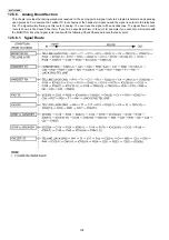
12.5.5. Digital Board Section
When the unit fails to boot up the system, take the troubleshooting procedures very carefully. It may have a serious problem.
The symptom: No response when the power is turned on. (No LCD display, and keys are not accepted.)
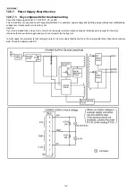
The first step is to check the power source. If there is no problem with the power supply unit, the problem may lie in the digital
unit (main board).
As there are many potential causes in this case (ASIC, DRAM, etc.), it may be difficult to specify what you should check first. If
a mistake is made in the order of checks, a normal part may be determined faulty, wasting both time and money.
Although the tendency is to regard the problem as a serious one (IC malfunction, etc.), usually most cases are caused by solder
faults (poor contact due to a tunnel in the solder, signal short circuit due to solder waste).
Note:
1. Electrical continuity may have existed at the factory check, but a faulty contact occurred as a result of vibration, etc., during
transport.
2. Solder waste remaining on the board may get caught under the IC during transport, causing a short circuit.
Before we begin mass production, several hundred trial units are produced at the plant, various tests are applied and any mal-
functions are analyzed. (In past experiences, digital IC (especially DRAM and FLASH ROM) malfunctions are extremely rare
after installation in the product.)
This may be repaired by replacing the IC, (DRAM etc.). However, the real cause may not have been an IC malfunction but a sol-
dering fault instead.
Soldering faults difficult to detect with the naked eye are common, particularly for ASIC and RA (Resistor Array). But if you have
an oscilloscope, you can easily determine the problem site or IC malfunction by checking the main signal lines.
Even if you don’t have such a measuring instrument, by checking each main signal line and resoldering it, in many cases the
problem will be resolved.
An explanation of the main signals (for booting up the unit) is presented below.
Don’t replace ICs or stop repairing until checking the signal lines.
An IC malfunction rarely occurs. (By understanding the necessary signals for booting up the unit, the “Not Boot up”
display is not a serious problem.)
What are the main signals for booting up the unit?
The ASIC (IC1) controls all the other digital ICs. When the power is turned on, the ASIC retrieves the operation code stored in
the FLASH ROM (IC2), then follows the instructions for controlling each IC. All ICs have some inner registers that are assigned
to a certain address.
It is the address bus by which the ASIC designates the location inside each IC. And the data bus reads or writes the data in
order to transmit the instructions from the ASIC to the ICs.
These signal lines are all controlled by voltages of 3.3V (H) or 0V (L).
Summary of Contents for KX-FT932BR-B
Page 11: ...11 KX FT932BR B 6 Technical Descriptions 6 1 Connection Diagram ...
Page 21: ...21 KX FT932BR B 6 4 2 Block Diagram ...
Page 23: ...23 KX FT932BR B ...
Page 61: ...61 KX FT932BR B 11 2 2 Service Mode Example of a printed out list ...
Page 67: ...67 KX FT932BR B ...
Page 68: ...68 KX FT932BR B CROSS REFERENCE Test Mode P 54 ...
Page 69: ...69 KX FT932BR B CROSS REFERENCE Test Mode P 54 ...
Page 70: ...70 KX FT932BR B CROSS REFERENCE Test Mode P 54 ...
Page 71: ...71 KX FT932BR B ...
Page 73: ...73 KX FT932BR B ...
Page 74: ...74 KX FT932BR B ...
Page 75: ...75 KX FT932BR B CROSS REFERENCE Test Mode P 54 ...
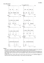
Page 102: ...102 KX FT932BR B NG Wave pattern Note Refer to NG Example P 107 ...
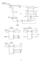
Page 104: ...104 KX FT932BR B I O and Pin No Diagram ...
Page 106: ...106 KX FT932BR B ...
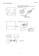
Page 107: ...107 KX FT932BR B 12 5 5 3 NG Example ...
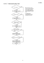
Page 111: ...111 KX FT932BR B 12 5 7 2 Troubleshooting Flow Chart ...
Page 116: ...116 KX FT932BR B 12 5 11 Thermal Head Section Refer to Thermal Head P 22 ...
Page 117: ...117 KX FT932BR B 13 Service Fixture Tools ...
Page 120: ...120 KX FT932BR B 14 2 Disassembly Procedurel 14 2 1 How to Remove the Operation Panel Block ...
Page 121: ...121 KX FT932BR B 14 2 2 How to Remove the Operation Board LCD and Platen Roller ...
Page 122: ...122 KX FT932BR B 14 2 3 How to Remove the Separation Holder and Document Feed Support ...
Page 123: ...123 KX FT932BR B 14 2 4 How to Remove the Image Sensor CIS and Feed Roller ...
Page 124: ...124 KX FT932BR B 14 2 5 How to Remove the Lock Lever and Thermal Head ...
Page 125: ...125 KX FT932BR B 14 2 6 How to Remove the Bottom Frame ...
Page 128: ...128 KX FT932BR B 14 2 10 Installation Position of the Lead Wires ...
Page 134: ...134 KX FT932BR B 15 2 3 Mechanical Movements in the Main Operations 15 2 3 1 Idle Status ...
Page 136: ...136 KX FT932BR B 15 2 3 4 Copying CROSS REFERENCE Sensor Section P 114 ...
Page 140: ...140 KX FT932BR B 16 1 4 Power Supply Board ...
Page 143: ...143 KX FT932BR B 16 3 Test Chart 16 3 1 ITU T No 1 Test Chart ...
Page 144: ...144 KX FT932BR B 16 3 2 ITU T No 2 Test Chart ...
Page 145: ...145 KX FT932BR B MEMO ...
Page 152: ...152 KX FT932BR B MEMO ...
Page 161: ...161 KX FT932BR B MEMO ...
Page 163: ...163 KX FT932BR B 20 1 2 Upper Cabinet Section ...
Page 164: ...164 KX FT932BR B 20 1 3 Lower Cabinet Section ...
Page 165: ...165 KX FT932BR B 20 1 4 Gear Block Section ...
Page 166: ...166 KX FT932BR B 20 1 5 Screws ...
Page 167: ...167 KX FT932BR B 20 1 6 Accessories and Packing Materials ...

