– 6-18 –
22. Stick KEYPAD SPONGE, fix the KEYPAD CABLE and assemble MIC.
23. Put RECEIVER RUBBER and Insert PCBA to the MIDFRAME.
24. Make PCBA hooked in MIDFRAME well.
Page 1: ... MHz 1900 MHz Tx Frequency Range 880 915 MHz 1710 1785 MHz 1850 1910 MHz Rx Frequency Range 925 960 MHz 1805 1880 MHz 1930 1990 MHz Tx Rx separation 45 MHz 95 MHz 80 MHz RF Channel Bandwidth 200 kHz Number of RF channels 174 374 300 Speech coding Full rate Enhanced Full rate Operating temperature 10 C to 55 C Type Class 4 Handheld Class 1 Handheld Class 1 Handheld RF Output Power 32 dBm maximum 29...
Page 2: ...NTS 1 INTRODUCTION 1 1 1 1 Purpose of the Manual 1 1 1 2 Structure of the Manual 1 1 1 3 Servicing Responsibilities 1 1 2 GENERAL DESCRIPTION 2 1 2 1 General 2 1 2 2 Features 2 1 2 3 Handportable Main Kits 2 1 3 OPERATING INSTRUCTIONS 3 1 3 1 General 3 1 3 2 Liquid Crystal Display 3 1 3 3 Location of Controls 3 2 3 4 Concept of Operation 3 3 3 5 Alpha Entry 3 4 3 5 1 Character Set Key Assignments ...
Page 3: ...scriber Identity Module SIM 5 8 5 3 5 CPU Memory 5 9 5 3 6 LCD 5 9 5 3 7 Real Tim Clock RTC 5 9 5 3 Audio System 5 10 5 3 1 Voiceband Baseband Codec 5 10 5 3 2 Microphone 5 11 5 3 3 Receiver 5 12 5 3 4 Loud Speaker 5 12 5 4 Power Management Subsystem 5 13 5 4 1 Power Source 5 13 5 4 2 Regulator Control 5 13 5 4 3 Voltage Regulation 5 13 5 5 Battery Charging and Monitoring 5 15 5 5 1 Charging Curre...
Page 4: ...ocedure 8 5 8 3 4 Enter Test 8 5 8 3 5 TX Test 8 6 8 3 6 RX Test 8 9 8 3 7 Battery 8 11 9 REPLACEMENT PARTS LIST 9 1 9 1 Exploded View 9 1 9 2 Case and Cover Parts List 9 2 9 3 Main PCB 9 3 10 BLOCK DIAGRAM 10 1 10 1 Baseband 10 1 10 2 RF Band 10 2 11 CIRCUIT DIAGRAM 11 1 11 1 Baseband 11 1 11 2 RF Band 11 2 11 3 Analogue Baseband and Power Management 11 3 11 4 LCD and Camera 11 4 12 LAYOUT DIAGRA...
Page 5: ... Telephone system operating on GSM Digital Cellular Networks 1 2 Structure of the Manual 1 3 Servicing Responsibilities The manual is structured to provide service engineering personnel with the following information and procedures 1 General and technical information provides a basic understanding of the equipment kits and options together with detailed information for each of the major component ...
Page 6: ...ovided Dual Codec which includes Full Rate and Enhanced Full Rate EFR Speech Codec Triple Band E GSM 900 and PCS 1800 1900 operation Tegic T9 Text Entry Voice Ringer Desktop handsfree function comprising integral echo cancellation and noise suppression Wireless Application Protocol WAP Browser Backup Battery Downloadable polyphonic melody ring tones Clock Calculator and Currency Converter 2 3 Hand...
Page 7: ... Figure 3 1 Liquid Crys tal Dis play S tatus Icons Icon Description The received signal strength indication Ð No CHPS Line1 Line2 Indicated the battery level Low Battery Displayed when the user is registered to a non home network roaming Displayed when call divert is enabled ÐNo CPHS Line1 Line2 Line1 Line2 Displayed when phone lock is enabled Displayed when an unread message is store or lights wh...
Page 8: ... 3 2 3 3 Location of Controls Receiver Display Phone Jack Charger Connection The Phone Jack can be used as data transmission port to perform download and test tasks ...
Page 9: ... functions indicated by text shown on the LCD screen In idle long press left soft key to enter Messages long press right soft key to enter Profile Mode List Numeric key pads Long Press to enter a or P When you need to dial an extension number dial the phone number firstly then long press to add a P and enter the extension number Send Answer Key Make a call or answer a call In idle mode check the l...
Page 10: ...TC T9 on T9 Abc T9 abc T9 ABC T9 Abc T9 abc T9 ABC 123 BPMF T9 Abc T9 abc T9 ABC 123 BPMF 123 BPMF Send SC Thai T9 off T9 on T9 off Abc abc ABC 123 BPMF T9 off Abc abc ABC 123 Thai a A d D g G j J m M p P t T w W b B e E h H k K n N q Q u U x X c C f F i I l L o O r R s S v V y Y StrokeTC StrokeTC StrokeTC StrokeTC 8 StrokeSC Stroke_S StrokeSC StrokeSC 7 PinYin PinYin PinYin PinYin Key 1 2 3 4 5 6...
Page 11: ... Memory status My Numbers Hotkey dial My Contacts Shortcuts Defaults Game Puddieland Quadball Exode Contacts Alerts Profiles Normal Quiet Outdoors Headset Meeting Customer Any key answer On Off Auto key lock On Off Sounds Volume Ringtones Keytone Warning tone Warning Shutter sound Shutter sound Language T9 Input Display Ianguages Browser Video Camera Camera Create Inbox Outbox User Messages Memory...
Page 12: ...rmation is restricted to those operations supported by the telephone The and in the following procedures should be replaced by and respectively Also SND and END should be replaced with and keys MEMORY LOCATION Leading zeros can be left out of the location number e g 007 can be 7 0 6 Change PIN 0 4 OLD PIN NEW PIN NEW PIN Change PIN2 0 4 2 OLD PIN2 NEW PIN2 NEW PIN2 Unblock PIN 0 5 PIN UNBLOCKING K...
Page 13: ...ONE NUMBER SND Teleservice Bearer Service Service MMI Service Code All teleservices 10 Telephony 11 All data teleservices 12 Facsimile services 13 Short Message Service SMS 16 All teleservices except SMS 19 Voice group service 17 Service MMI Service Code All bearer services 20 All asynchronous services 21 All synchronous services 22 All data synchronous services 24 All data asynchronous services 2...
Page 14: ...ICATION SERVICE SND Status SERVICE CODE TELECOMMUNICATION SERVICE SND Clear all Call Diverts 002 Call Bar Type Service Code All outgoing calls 33 Outgoing International calls 331 Outgoing International calls except those to the PLMN 332 All incoming calls 35 Incoming international calls when roaming 351 Set PASSWORD TELECOMMUNICATION SERVICE SND Clear TELECOMMUNICATION SERVICE SND Status TELECOMMU...
Page 15: ... Security Call bar Calls cannot be made The telephone is not registered to a network Move to a coverage area and operate the telephone after it has registered with a network Calls cannot be made from Fixed Dial Store Check that SIM supports Fixed Dial Check if the Fixed Dial is switched on Phone Operation Security Fixed Dial Check the telephone number is stored in the Fixed Dial The telephone is n...
Page 16: ...validated The PIN2 is blocked permanently because the wrong PUK2 has been entered 10 times Services controlled by PIN2 cannot be used Contact the Service Provider Warning Store Full Continue The message area is full New messages cannot be stored unit some of the currently stored messages are deleted Code Type Number or Digits Description Personal Identification Number PIN 4 to 8 Controls SIM secur...
Page 17: ... Personal Identification Number used for SIM security Supplied by the service provider PIN2 Personal Identification Number used for the control of Fixed Dial Memory and call charge metering Supplied by the service provider PUK PUK2 PIN PIN2 Unblocking Key Used to unblock the PIN PIN2 Supplied by the service provider Registration The act of locking on to a GSM network This is usually performed auto...
Page 18: ...ffset from Centre Frequency kHz Offset from Centre Frequency kHz Maximum Level Relative to Carrier dB Maximum Level dBm 100 0 5 200 30 250 33 400 60 600 to 1800 60 4 1 4 Output RF Spectrum due to Switching Transients E GSM 900 GSM 1800 400 19 22 22 600 21 24 24 1200 21 24 24 1800 24 27 27 GSM 1900 Measurement conditions for output RF spectrum measurements Frequency Span 0 Hz Measurement Bandwidth ...
Page 19: ...Hz 300 kHz 36 36 500 MHz to 1 GHz 0 to 1 MHz 100 kHz 300KHz 36 36 1 GHz to 12 75 GHz Excl relevant TX band E GSM 880 MHz to 915 MHz DCS 1710 MHz to 1785 MHz and the Rx bands 925 MHz 960 MHz 1805 MHz 1880 MHz 0 to 10 MHz 10 MHz 30 MHz offset from edge of relevant Tx band 100 kHz 300 kHz 3 MHz 300 kHz 1 MHz 3 MHz 30 30 30 30 1 0 GHz 1 710 GHz 36 1 710 GHz 1 785GHz 30 1 785 GHz 12 75GHz Relevant TX b...
Page 20: ... condition but must remain the same for FER and class 1b RBER measurements for the same channel condition Channels Propagation Conditions TU high Propagation Conditions RA Propagation Conditions HT Static Conditions Test Limit error rate Minimum No of samples Test Limit error rate Minimum No of samples Test Limit error rate Minimum No of samples Test Limit error rate Minimum No of samples TCH FS F...
Page 21: ...FR 600 kHz to FR 800 kHz FR 800 kHz to FR 1 6 MHz FR 1 6 MHz to FR 3 MHz 915 MHz to FR 3 MHz FR 3 MHz to FR 980 MHz FR 600 kHz to FR 800 kHz 1 785 MHz to FR 3 MHz 835 MHz to 915 MHz 980 MHz to 1 000 MHz 100 KHz to 835 MHz 1000 MHz to 12 75 GHz 100 kHz to 1 705 MHz 1 705 MHz to 1 785 MHz 1 920 MHz to 1 980 MHz 1 980 MHz to 12 75 GHz 70 70 80 90 90 113 113 90 90 70 70 80 87 87 113 101 101 90 GSM 190...
Page 22: ...Hz 1 930 MHz 1 990 MHz RX Bandwidth 35 MHz 75 MHz 60 MHz TX Bandwidth 35 MHz 75 MHz 60 MHz Number of Channels 174 374 299 AFRCN Channel Numbers 0 124 512 885 512 810 975 1023 1st TX Channel 880 2 MHz 1 710 2 MHz 1 850 2 MHz Ch 975 Ch 512 Ch 512 Last TX Channel 914 8 MHz 1 784 8 MHz 1 909 8 MHz Ch 124 Ch 885 Ch 810 1st RX Channel 925 2 MHz 1 805 2 MHz 1 930 2 MHz Ch 975 Ch 885 Ch 512 Last RX Channe...
Page 23: ... DIV TLCPO VCPO UVTUNE TXVCO 26 MHz VCTCXO DIV 90 PA PA RXI RXI RQI RQI TXI TXI TQI TQI T H DATA CLKL FREF DC O C LNA900IN LNA1800IN LNA1900IN Σ FRAC N PLL DC O C DC O C Σ LOG EN LOG EN U1101 U1201 RF Transceiver with Power Ramping Controller Integrated Crystal Oscillator for Multi Band GSM GPRS and EDGE Applications ...
Page 24: ... MHz General Antenna EB X300 uses a Helical type monopole antenna which is optimised for operation on GSM DCS and PCS bands RF circuit design is built based on the direction conversion transceiver IC integrated by SAW filters U1201 power amplifier with control circuit and Transmitter receiver switch RF LO always requires external frequency sources with VCTCXO The LO is frequency is adjusted period...
Page 25: ...equency up conversion with high output spectral purity The clock source is 26 MHz VCTCXO external instead of XTAL function block active The VCTCXO provides an external clock source which is more stable over extreme temperature conditions than an internal clock It has a power saving function in standby mode Transceiver Transmitter Base band section Antenna 3 wire bus TX IN TX IN I Q PAVAPC VAPC Ban...
Page 26: ...rrection loop ensures DC offsets generated in the U1201 do not overload baseband chain The receiver can be calibrated to optimise IP2 performance which ensures limited baseband interfering signal amplitude The U1201 also features an integrated fully programmable sigma delta fraction N synthesiser suitable for GPRS multi slot operation Transceiver Receiver RX LO source from chip Figure 5 4 Receiver...
Page 27: ...l Baseband Processor Keyboard R F Block BBCLK Vibrator U102 Memory Flash SRAM 128MB 32MB RTC Crystal MIC Speaker SIM Socket Keypad Data Bus CLKIN OSC 32 768 kHz DataBus Address Bus LCDControlBus A B C Serial Port RFControlBus GPIO4 USCDataBus SIM Interface VCC VBAT VMEM TXIQ RXIQ Control Signal VMEM Handfree Input HANDFREEIN GPIO34 Receiver VMEM VRTC VSIM Buffer VVCXO 26MHz_BB VOUTNORP N 3 in 1 Ph...
Page 28: ... and 16K word Program SRAM 4K word Program Instruction Cache Architecture supports Full Rate Enhanced Full Rate Half Rate and AMR Speech Encoding Decoding Algorithms 3 Peripheral Subsystem including Shared Peripheral Bus and Interface Peripherals Figure 5 6 U101 Functional Block Diagram UNIVERSAL SYSTEM CONN INTERFACE SPI INTERFACE CHANNEL CODEC SIM INTERFACE USB INTERFACE U101 only VOICEBAND BASE...
Page 29: ...e is designed to support a 3 V SIM card The nominal 2 85 V supply VSIM for the SIM interface is provided by U201 0x00 SMSMR SIM Character Mode Register Read Write 0x02 SMBRR SIM Bit Rate Register Read Write 0x04 SMSCR SIM Control Register Read Write 0x06 SMTDR SIM Data Transmit Register Read Write 0x0A SMRDR SIM Data Receive Register Read Write 0x08 SMSSR SIM Status register Read Write 0x0C SMSCMR...
Page 30: ...river the nDISPLAYCS line is used for chip select LCD_CTL is set high to send data and set low to send commands Clock functions are provided by a Real Time Clock built into U101 The module is synchronised by a 32 768 kHz crystal and has a backup power source provided by a capacitor U101 has a clock auto compensation function to take into account any inaccuracies of the crystal This is able to cali...
Page 31: ...sed in normal receiver mode Voiceband auxiliary output is used in earpiece receiver mode Buzzer output signal via a melody IC is used in loud speak mode The voiceband input is used for microphone connection and the auxiliary input used for external Handsfree microphone connection 5 3 1 Voiceband Baseband Codec Chipset U201 Package 148 Ball LFBGA Feature Baseband Transmit Section GMSK Modulator I c...
Page 32: ...des seven regulator outputs for VCORE 1 8V VMEM 2 93V VEXT 2 93V VRTC 1 8V VCTCXO 2 75V VSIM 2 85V VMIC 2 75V VCORE and VMEM provide all digital power and VMEM provides all analogue power VRTC is used to charge Li Mn coin cell for real time clock and VCTCXO is the power source of 13MHz clock buffer U101 also provides the charge pump and hardware reset Mic Filter Filter Filter Filter Tone Battery C...
Page 33: ...with a Type 3 2 artificial ear 1 1 dB 0 dB 3 dB 2 2 dB 0 dB 0 dB 3 5 dB 0 dB 3 dB 4 5 dB 6 dB 9 dB A second speaker is mounted in the rear case for DTHF operation Ring tones and melodies are played via the loudspeaker The volume level of ring tones is defined by the 6 bit PWM register setting in U201 5 3 3 Receiver 5 3 4 Loudspeaker Volume Level PGA Volume Total Gain 5 0 5 10 15 1 000 10 000 100 F...
Page 34: ...he battery is not in Deep Discharge Lockout Under Voltage Lockout or Thermal Shutdown the Real Time Clock regulator and the reference are always enabled The other regulators are enabled or disabled based on input from the user or software If the user presses the power on key KEYON the regulators required to boot the software are enabled If a charger is detected CHGDET the regulators required to bo...
Page 35: ...pacitor type backup coin cells to run the real time clock module The RTC LDO supplies current both for charging the coin cell and for the RTC module In addition it features a very low quiescent current since this LDO is running all the time even when the handset is switched off It also has reverse current protection with low leakage which is needed when the main battery is removed and the coin cel...
Page 36: ...itted the charging algorithm is determined by constant voltage and constant current control with time temperature and voltage safeguards 5 5 2 Deeply Discharged Batteries In the case of deeply discharged batteries there may not be enough power in the battery to initiate charging In this case the charging circuit automatically starts to trickle charge the battery until there is enough power to swit...
Page 37: ... USC3 USC3 Bottom I O TP134 BB USC4 USC4 Bottom I O TP135 BB USC5 USC5 Bottom I O TP136 BB USC6 USC6 Bottom I O TP137 BB GPIO_13 UNUSED Bottom I O TP140 BB VSIM SIM VCC Voltage Bottom P TP141 BB SIMRST SIM RESET Bottom I TP142 BB SIMCLK SIM CLOCK Bottom O TP143 BB SIMDATAIO SIM Data I O Bottom I O TP157 BB INT_ABB AD6537B INTERRUPT Bottom O TP158 BB GPIO_55 BOOT SETTING Bottom I O TP161 BB GPIO_7 ...
Page 38: ...34 TP130 TP135 TP402 TP139 TP115 TP132 TP163 TP161 TP162 TP137 TP138 TP110 TP168 TP133 TP136 TP112 TP151 TP210 TP211 TP240 TP241 TP111 TP143 TP142 TP140 TP141 TP158 TP113 TP157 TP131 TP150 TP214 TP403 TP213 TP520 TP341 TP340 TP230 TP170 TP302 TP301 TP303 TP164 TP114 TP160 TP160 TP169 TP144 TP159 TP152 TP165 TP166 ...
Page 39: ...round point Wrist Strap A QUICK RELEASE SKIN CONTACT DEVICE WITH A FLEXIBLE CORD WHICH HAS AN INTEGRAL SAFETY RESISTOR OF BETWEEN 5 2 kΩ AND 1 2 MΩ SHALL BE USED Containers All containers and storage must be of the conductive type WARNING The equipment described in this manual contains polarised capacitors utilising liquid electrolyte These devices are entirely safe provided that neither a short c...
Page 40: ... 6 2 6 2 Disassembly 1 Remove the BATTERY COVER and BATTERY 2 Unscrew the three screws on BASE CASE 3 Gently dismount RECEIVER COVER from TOP CASE ...
Page 41: ...4 Unscrew the two screws located on TOP CASE 6 Remove the LCD rear case Open the LCD connector cover and then disconnect the LCD cable 5 Open the LCD panel and then unscrew the five screws 6 3 ...
Page 42: ...sert the separation tool into gap and gently slide the tool in the directions shown ensuring that the case hooks separate along each edge 8 Open the CMOS connector cover and then withdraw the CMOS CABLE Use tools to separate MIDFRAME and BASE CASE along both sides 6 4 Midframe Top case ...
Page 43: ...Spread the Base case and Midframe and then remove them TAKE GREAT CARE NOT TO DAMAGE THE CMOS CABLE WHEN SEPARATING THE BASE CASE AND MIDFRAME 10 Take out COMS module from MIDFRAME 6 5 Midframe Base case ...
Page 44: ...11 Lift PCBA by loosening the hook in the right upper side 12 Loosen two hooks on the backside of MIDFRAME to take out PCBA completely 6 6 13 Take out MIC from MIDFRAME ...
Page 45: ...14 Take out KEYPAD SHIELD 15 Take out CABLE KEYPAD ASSY 6 7 16 Take out VIBRATOR ...
Page 46: ...17 Take out the SPEAKER from BASE CASE 18 Take out the BASE CASE SPRING 6 8 19 Dismount ANTENNA COVER carefully ...
Page 47: ...20 Dismount ANTENNA COVER carefully 21 The ANTENNA TAPE can be replaced 6 9 22 Remove two LCD MYLARS ...
Page 48: ...efully to pull out the LCD HINGE then takes out LCD CASE 6 10 25 Take out LCD STOPPER Note Because of the strong adherence between LCD LENS and LCD BASE and dust concer we recommend you replace the LCD LENS BASE SP ASSY instead of individual part if needed ...
Page 49: ... 6 11 6 3 Reassembly 1 Insert HINGE into LCD LENS BASE ASSY 2 Hook LCD HINGE SPRING to the TOP CASE 3 Adjust the HINGE direction to insert into TOP CASE ...
Page 50: ... 6 12 4 Bend the TOP CASE slightly to put HINGE STOPPER 5 Re bend the TOP CASE carefully to normal condition 6 Place LCD and insert LCD CABLE from the gap and connect to LCD ...
Page 51: ... 6 13 7 Insert two LCD MYLARS 8 Assemble LCD REAR CASE and tighten four SCREWS 9 Stick ANTENNA TAPE on ANTENNA COVER SCREW 1 6 3 5 X4 ...
Page 52: ... 6 14 10 Assemble ANTENNA COVER to BASE CASE 11 Stick ANTENNA TAPE on BASE CASE and position well 12 Assemble SPEAKER and BASE SPRING ...
Page 53: ... 6 15 13 Combine COMS with CMOS BASE ASSY 14 Cover CMOS SHIELD 15 Close the COMOS door and fix COMS ASSY in the BASE CASE ...
Page 54: ... 6 16 16 Assemble VIBRATOR to MIDFRAME 17 Stick CABLE KEYPAD ASSY including both sides 18 Position the cable connector in the two fixed points in the back of MIDFRAME ...
Page 55: ... 6 17 19 Hook KEYPAD SHIELD and position the branches properly 20 Stick the KEYPAD COPPER along the back edge 21 Stick the KEYPAD COPPER on the front KEYPAD SHIELD ...
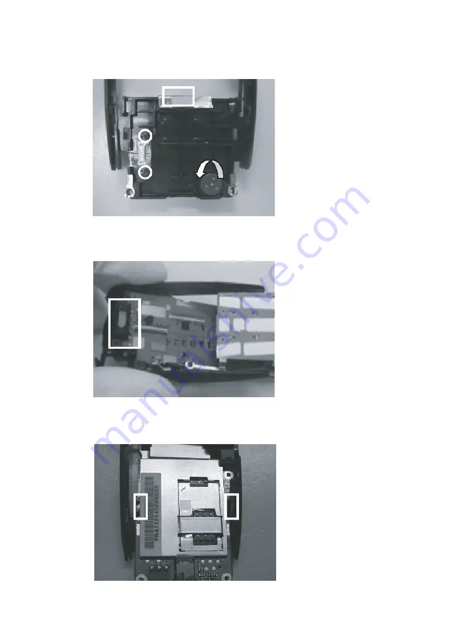
Page 56: ... 6 18 22 Stick KEYPAD SPONGE fix the KEYPAD CABLE and assemble MIC 23 Put RECEIVER RUBBER and Insert PCBA to the MIDFRAME 24 Make PCBA hooked in MIDFRAME well ...
Page 57: ... 6 19 25 Insert CMOS CABLE from the gap and assemble PCBA with BASE CASE Then connect CMOS to PCBA 26 Assemble TOP CASE and MIDFRAME 27 Tighten one screw Torque 0 5 0 05 Kgf cm SCREW 1 6 3 5 X1 ...
Page 58: ...8 Tighten two screws on the top Torque 0 5 0 05 Kgf cm 29 Fix the RECEIVER COVER on TOP CASE 30 Tighten three screws on the BASE CASE and insert CARKIT RUBBER SCREW 1 6 5 2 X2 SCREW 1 6 3 5 X1 SCREW 1 6 5 2 X2 ...
Page 59: ...3 External testing describes equipment requirements and general set up procedure Section 7 4 Complete Unit Test Setup Describes how the items of test equipment are used together and general set up procedure Adjustment Procedures are described in Section 8 CAUTION The Printed Circuit Board PCB used in this telephone has been manufactured using Lead Free solder SPARKLE ECO SOLDER Part No ESC F3 M705...
Page 60: ...repair jig dummy battery and external power supply Figure 7 3 Power Cable The RF cable provides the necessary connections between the PCB Repair Jig RF Adapter and external test equipment RF Cable Part No 3WZ001103AAA The Download Cable is used for software download and TX Power RX RSSI calibration with dummy battery Download Cable Part No DD0VE2TH004 ...
Page 61: ... software for the telephone unit and should be installed onto the personal computer to be used for testing Calibration Software GSM Tester Figure 7 5 PCB Repair Jig The PCB Repair Jig provides the necessary connections between the PCB Assembly and external test equipment It is required for RF calibration The dummy battery provides the interface to supply power via power cable It has been contoured...
Page 62: ...uter with RS232 interface and running Microsoft Windows 95 98 XP or 2000 7 GSM test station 8 EB X300 Service software The EB X300 Service software should be installed onto the main drive of the personal computer The RF cable is connected to the GSM test station via a suitable adaptor The 3 8 V supply is connected to the RF Adaptor and PCB Repair Jig using the power cable NOTE A suitable test SIM ...
Page 63: ...ftware Upgrade Equipment setting for single downloading 1 Connect the handset to the test equipment Run PAC_DLTool_v4 5 2 Chek that the handset is switched off Ensure that the correct target file mbf is available and ready to use RS232 Handset Download Cable PC ...
Page 64: ...lick on the wheel icon and select the target file 3 Ensure the EB X300 checkbox is checked Check the following boxes as required Keep FFS Keep user data if no structure modification Keep Media FFS Keep user media data if no structure modification 4 Long press on the power key and follow the indication on screen The progress status will be shown on screen 5 If any failure occurs click on the releva...
Page 65: ... Green Red RGB 3 Software Version Check the current software version Software Version Mapping Version LP Version 4 Auto answer Valid setup when insert test SIM 5 Camera to active the camera function 6 Defect Cancellation close the CMOS door and cover with black shelter first Choose this item and press shutter key then wait Success message showing OK to exit 7 DTMF On Determine if DTMF function val...
Page 66: ...r Scaling Factors TX Freq Compensation B RX RSSI Received Signal Strength Indication Accurate Gain Control RX Freq Compensation C Battery Calibration 8 3 2 Main Subjects ARFCN Absolute Radio Frequency Channel Numbers Band TX Fu n RX Fl n ARFCN E GSM900 Fu n 890 0 2 n Fl n Fu n 45 0 n 124 Fu n 890 0 2 n 1024 975 n 1 023 Middle 37 DCS1800 Fu n 1 710 2 0 2 n 512 Fl n Fu n 95 512 n 885 Middle 698 PCS1...
Page 67: ...edure 8 3 4 Enter Test Execute the main program PAC CalTool V4 4 exe 1 Select the relevant PORT and MODEL 2 Click ENTER TEST MODE 3 If successful a dialogue box will pop up within 3 seconds Click on OK to continue PAC Tool V4 4 X300 ...
Page 68: ...olerances dbm Normal Extreme 29 30 31 0 1 2 3 4 5 6 7 8 9 10 11 12 13 14 15 28 36 34 32 30 28 26 24 22 20 18 16 14 12 10 8 6 4 2 0 2 3 3 3 3 3 3 3 3 3 3 3 4 4 4 4 4 5 5 2 5 4 4 4 4 4 4 4 4 4 4 4 5 5 5 5 5 6 6 PCS 1900 Power Control Level Transmitter Output Power Tolerances dbm Normal Extreme 22 29 30 31 0 1 2 3 4 5 6 7 8 9 10 11 12 13 14 15 16 21 Reserved 33 32 30 28 26 24 22 20 18 16 14 12 10 8 6...
Page 69: ...Y for AFRCN 7 Click APPLY for scaling factor 8 Read power level on test set 9 Adjust scaling factor to nominal power 10 Copy scaling factor value to box 5 in the relevant table 11 Add scaling factor value to box 0 to 4 in table 12 Repeat 3 to 9 for DCS PCS 13 Copy scaling factor value to box 0 in the relevant table 14 Copy scaling factor to correct location in table 15 Click WRITE response NVRAM W...
Page 70: ...in the same channel 3 Enter the estimate value in SCALING FACTOR click APPLY and read the TX output power value on the tester Repeat until the TX power is within the allowed range 4 Enter the ideal scaling factor in the corresponding cell of SF column 5 Repeat step 2 to 4 until ALL 9 channels are down 6 Click WRITE to adjust the handset in the end 1 2 3 6 4 ...
Page 71: ... GSM etc 3 Set test set ARFCN 37 AMP 60dbm FREQ 0 0667 MHz 4 Click SEND 5 Click OFFSET in GSM 6 Set test set for DCS 1800 ARFCN 698 7 Set ARFCN to 698 8 Repeat 4 and 5 OFFSET in DCS 9 Set test set for PCS 1900 ARFCN 661 10 Set ARFCN to 661 11 Repeat 4 and 5 OFFSET in PCS 12 Click WRITE response NVRAM WRITE OK 13 Cycle power on handset 14 Re ENTER TEST MODE 8 3 6 RX Test 2 4 1 12 5 ...
Page 72: ...or ARFCN 4 Click SEND 5 Copy RSSI value to corresponding box 6 Repeat 2 to 5 for other GSM DCS bands Select PCS 8 Repeat 2 and 5 9 Click WRITE response NVRAM WRITE OK 3 times 10 Cycle power on handset Set tester as a Test Function CW b RF Gen Power 60dBm c MS TX Level 5 5 1 2 4 9 ...
Page 73: ...ry adjustment NOTES 1 Change the handset comport setting before starting Press 369 Com port GENIE 2 On completion of Battery Adjustment set the comport back to Off otherwise the handset may malfunction Operation Process 1 Set power supply to 4 2V DC and click ADC to read Check if the value is in the range 2 Set power supply to 3 2V DC and click ADC to read Check if the value is in the range Power ...
Page 74: ...ed View B TOP CASE ASSY C BASE CASE ASSY A LCD LENS BASE SP ASSY AB LCD TOP CASE SP ASSY 5 7 6 41 41 40 40 41 41 40 40 40 40 42 9 19 20 22 23 34 33 32 31 30 24 25 27 28 29 26 21 11 11 1 2 12 13 15 16 18 14 17 3 4 SH K SH R SH S 35 38 36 39 37 ...
Page 75: ...13 KEY COPPER 16 GBRA1011011 KEY SPONGE 17 DD0RA1KP009 CABLE ASSY KEYPAD 18 GARA1002011 RECEIVER RUBBER 19 EERA1001019 KEYSET EN EERA1001027 KEYSET STROKE EERA1001035 KEYSET BPMF EERA1001043 KEYSET RUSSIA 20 AY010331046 MOTOR 21 1MIZZZZ08T3 MIC RUBBER 22 GARA1001015 MIC RUBBER 23 DN0B613S003 MIC 24 37RA1CAPA04 CMOS DOOR ASSY 25 1MIZZZZ08S5 CMOS ASSY 26 FBRA1010015 CMOS SHIELD 27 DN001518007 SPK Re...
Page 76: ... C320 CH31003KB11 CERAMIC CAPACITOR 0 01UF 16V C321 CH31003KB11 CERAMIC CAPACITOR 0 01UF 16V C322 CH5474KEA06 CERAMIC CAPACITOR 4 7UF 25V C330 CH01806JB07 CERAMIC CAPACITOR 18PF 50V C331 CH04706JB01 CERAMIC CAPACITOR 47PF 50V C332 CH01806JB07 CERAMIC CAPACITOR 18PFF 50V C334 CH41002KB93 CERAMIC CAPACITOR 0 1UF 10V C335 CH01806JB07 CERAMIC CAPACITOR 18PF 50V C336 CH01806JB07 CERAMIC CAPACITOR 18PF ...
Page 77: ...C CAPACITOR 15PF 50V C1271 CH 5006TB07 CERAMIC CAPACITOR 0 5PF 50V C1272 CH 5006TB07 CERAMIC CAPACITOR 0 5PF 50V C1296 CH21006JB10 CERAMIC CAPACITOR 1000PF 50V C1297 CH41002KB93 CERAMIC CAPACITOR 0 1UF 10V CON301 DFHD03MS240 CONNECTOR 3P Battery Connector D301 BC0CRS03Z09 DIODE CRS03 30V 1A SCHOTTKY D302 BDDZS56BZ09 DIODE ZENER UDZS5 6BTE 17 5 49 5 73V D303 BC0CRS03Z09 DIODE CRS03 30V 1A SCHOTTKY ...
Page 78: ...R 390Ω 1 16W R1205 CS15102FB01 FIXED RESISTOR 510Ω 1 16W R1206 CS05102JB01 FIXED RESISTOR 51Ω 1 16W R1207 CS01002JB06 FIXED RESISTOR 10Ω 1 16W R1210 CS00002JB03 FIXED RESISTOR 0Ω 1 16W R1211 CS51002JB05 FIXED RESISTOR 1M 1 16W R1212 CS00002JB03 FIXED RESISTOR 0Ω 1 16W R1221 CS33902FB08 FIXED RESISTOR 39K 1 16W R1222 CS01002JB06 FIXED RESISTOR 10Ω 1 16W R1223 CS01002JB06 FIXED RESISTOR 10Ω 1 16W R1...
Page 79: ...HANDFREEIN GPIO34 Receiver VMEM VRTC VSIM Buffer VVCXO 26MHz_BB VOUTNORP N 3 in 1 Phone Jack VOUTAUX P LOUD VINNORP N VINAUX P N TX RX TX RX Analogue Switch Voice Data GPIO2 AIN1P 1N AOUT1P 1N AIN2P 2N AOUT3P AOUT3N U201 GSM Analogue Baseband and Codec Power Management EXTPWR Li Ion Battery 3 in 1 Power Jack Over Voltage Protect Circuit PMOSFET Charging Circuit VBAT VCORE VMEM VEXT VSIM VRTC VABB ...
Page 80: ...XVCO 26 MHz VCTCXO DIV 90 PA PA RXI RXI RQI RQI TXI TXI TQI TQI T H DATA CLKL FRQ DC O C LNA900IN LNA1800IN LNA1900IN Σ FRAC N PLL DC O C DC O C Σ LOG EN LOG EN U1101 U1201 RF Transceiver with Power Ramping Controller Integrated Crystal Oscillator for Multi Band GSM GPRS and EDGE Applications ...
Page 81: ...GPO_7 TR_SW2 GPO_8 TR_SW1 GPO_9 TR_SW3 GPO_10 TR_SW4 GPO_11 GSM_ON GPO_16 DCS_ON GPO_17 GPO_18 SYNTHEN GPO_19 SYNTHDATA GPO_20 SYNTHCLK GPO_21 RXON GPO_0 TXON GPO_1 GPO_3 CLKOUT CLKOUT_GATE GPIO_32 GPO_5 GPO_6 ASDI ASDO ASFS BSDO BSOFS BSDI BSIFS GPIO_24 SIM ENABLE GND1 GND2 GND3 GND4 GND5 GND6 GND7 GND8 GND9 GND10 GND11 VCC2 VCC3 VCC4 VSIM VMEM1 VMEM2 VMEM3 VMEM4 VEXT01 VEXT02 VEXT03 VEXT04 VDDRT...
Page 82: ...25 5 6K R1223 10 R1224 10 R1222 10 C1298 NM U1261 SAFEJ942 IN 1 G 2 OUT 3 G 4 R1291 0R R1211 1M C1297 100n R1212 0R C1231 33n C1230 33n C1222 NM C1243 22p C1244 100n C1245 100n C1250 2 7p C1203 2 2n R1292 180 C1203 39p C1248 33p C1249 1n C1229 220p C1242 10U C1228 8 2n C1227 680p C1241 100n C1223 22p C1226 100n R1295 0R C1224 100n C1216 100n C1262 15p C1271 0 5p C1205 1n C1272 0 5p L1261 8 2n C121...
Page 83: ...M VSIM VRTC SGND AOUT2N SPWR AOUT2P LDOEN KEYOUT KEYON IBIAS AGND4 GND_NET1 GND_NET2 VBAT_NET VBATSENSE R245 510R C214 0 1U C228 4 7U C229 0 1U REFCHG VBAT C312 33p C311 0 1U C310 33p C211 1U TP302 TP_GND TP303 50 mils TP301 TP_VBAT CON301 BAT_CON 3 2 1 VBAT BAT_TEMP GND R311 10K 1 2 138 1 568 1 705 MICP MICN EXT_MIC AUXMICP AUXMICN VMIC C337 18p T330 1 2 MIC330 MIC GPAD MIC331 GND C338 47p C351 0...
Page 84: ...DCLK SCK GPIO0 T413 BZX884 1 2 J403 CMOS 26 25 24 23 22 21 12 11 10 9 8 7 6 5 4 3 20 19 18 17 16 15 13 14 2 1 ENB AVDD DVDDI SDA SCK GND GND VCLK DVDDC RESETB GND VSYNC HSYNC STRBE MCLK GND Y0 Y1 Y2 Y3 Y4 Y5 Y7 Y6 ID NC C424 12p J402 LCD CONN30 1 2 3 4 5 6 7 8 9 10 11 12 13 14 15 16 17 18 19 20 21 22 25 26 24 23 27 28 29 30 GND GND GND GND RES CS WR RD A0 GND GND D0 D1 D2 D3 D4 D5 D6 D7 GND GND VD...
Page 85: ...C373 C370 C311 C212 C211 C214 C224 C210 C631 C620 C215 C221 C1132 C222 C229 C1134 C1136 C1147 C1224 C1272 C227 C1231 C1230 C1221 C1262 C1215 C1214 C1216 C1211 C1271 C1143 C1149 C213 C223 C1296 C1297 C1298 C1226 C621 C1227 C1148 C1205 C1203 C1202 C651 C1145 C1139 C629 C1130 C335 C523 C241 C522 C521 C420 C520 C142 C144 C352 C332 C330 C377 C322 C351 C338 C339 C353 C337 C334 C331 C143 C240 C336 C376 C...