background image


5S-P-003   

Program Writer   


© Copyright 2022, PADAUK Technology Co. Ltd


Page 21 of 34 

5S-P-003-UM-EN-V007 

–  Oct.  14,  2022 


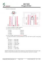
2.  Make the Connecting Board 


(1) 


Confirm the package pin of PMx131 MSOP-10   

(2) 


Confirm the JP7 pin in the back of Writer 

TA16-PA3 


TB16-PA0 

TA17-PA4 


TB17-PA7 

TA18-PA5 


TB18-PA6 

TA19-GND 


TB19-VDD 

(3) 


Put IC in SOCKET 

put IC from the

 fifth space

 of SOCKET 

According to the data below, connecting

VDD

GND

PA0

PA3

PA4

PA6

PA7

with IC

’s corresponding 

pins. 

TA16 (PA3) ----------TB7(IC-PA3) 

TA17 (PA4) ----------TB6(IC-PA4) 

TA18 (PA5) ----------TA6(IC-PA5) 

TA19 (GND) ----------TB4(IC-GND) 

TB16 (PA0) ----------TB5(IC-PA0) 

TB17 (PA7) ----------NC 

TB18 (PA6) ----------TA5(IC-PA6) 

TB19 (VDD) ----------TA4(IC-VDD) 

NOTICE: If the thirteenth group number (shift) is changed to 0, it means that the first pin of IC aligns the upper 

left first pin of Socket, at the same time all connection of corresponding IC pins have to be changed. 

Summary of Contents for 5S-P-003

Page 1: ...5S P 003 Program Writer User Manual Version 0 07 Oct 14 2022 Copyright 2022 by PADAUK Technology Co Ltd all rights reserved...

Page 2: ...Technology products are not warranted to be suitable for use in life support applications or other critical applications PADAUK Technology assumes no liability for such applications Critical applicati...

Page 3: ...rsion Update 14 3 1 Automatic update 15 3 2 Manual update 15 4 JUMPER Description 17 4 1 Examples 17 5 Connecting Board Making Description 18 5 1 Define the data of exclusive use packaged pin 18 5 2 C...

Page 4: ...Writer Copyright 2022 PADAUK Technology Co Ltd Page 4 of 34 5S P 003 UM EN V007 Oct 14 2022 9 2 Special notes of MTP On board writing 32 9 3 Special notes of voltage while On board or Multi Chip IC wr...

Page 5: ...CM signal table of chapter 7 6 Add 8 2 On line writing 0 05 2018 03 19 1 Update the address and telephone number of PADAUK Technology co Ltd 2 Update Partial pictures 3 Add description of O S check or...

Page 6: ...the exclusive power converter of Program Writer accessories Do not use other power converters to avoid damaging the Program Writer 3 Power Switch OFF ON 4 Buzzer Be used as alarm while failed to writ...

Page 7: ...d to use JP7 to transform relevant information About Connecting Board making please refer to chapter 5 3 Forced update mode button Forcing update the current version please refer to section 3 1 1 3 Th...

Page 8: ...application software and User Manual You can download the latest version of the application software at the following address including the latest version of the Program Writer http www padauk com tw...

Page 9: ...pyright 2022 PADAUK Technology Co Ltd Page 9 of 34 5S P 003 UM EN V007 Oct 14 2022 2 Functional Description A Engineering type B Simple type No matter simple type or engineering type they have the equ...

Page 10: ...e JUMPER position and IC placement would be prompted 4 The LCM also displays the messages and prompts synchronously 5 Users could also unplug the USB cable and write in alone mode after the file loade...

Page 11: ...ame content 2 4 Auto Program Start writing automatically It is equal to press the Program Writer s PROGRAM button The actions include Programmable check Program Verify Protect and so on When write suc...

Page 12: ...r Copyright 2022 PADAUK Technology Co Ltd Page 12 of 34 5S P 003 UM EN V007 Oct 14 2022 1 Click on Load File 2 Choose JP2_83K PDK click on 3 Confirm Download OK notice the message 4 Confirm the inform...

Page 13: ...Make sure the information IC Ready displayed on LCM 8 Click on Auto Program to start writing 9 Make sure the writing result is PASS 10 Make sure the information IC O K displayed on LCM 2 5 Rolling Cod...

Page 14: ...rting PDK file 3 Version Update You can download the latest version of the application software and Manual including the latest version of the Program Writer at the following address http www padauk c...

Page 15: ...am Writer version update 2 Click on OK to start updating 3 Download the new version in Program Writer 4 Verify the new version 5 Connect to PC automatically after finish NOTICE Please update manually...

Page 16: ...supply release the SW3 key enter the Boot loader mode FAIL light and OK light on at the same time the LCM displays the following information 3 Execute the writing application software and force the up...

Page 17: ...s an example SOP16 DIP16 standard package Jumper is placed in JP2 position which on the back of Writer and IC is placed in Textool no shifts As shown in the following pictures SOP14 standard package J...

Page 18: ...0F0 0x00F4 0 0x04 Grammar instruction Group Count Name Introduction Remarks 1 Pin Count the number of pin Up to 28 pins 2 VDD VDD pin number 3 PA0 PA0 pin number Note 1 4 PA3 PA3 pin number 5 PA4 PA4...

Page 19: ...l multi chip package pin set the corresponding bit value to zero 5 2 Connecting Board making The JP7 last 8 pins are writing pins as shown in the following figure While making a Connecting Board pleas...

Page 20: ...rks 1 Pin Count The number of package pin 10 2 VDD VDD pin serial number 1 3 PA0 PA0 pin serial number 9 4 PA3 PA3pin serial number 7 5 PA4 PA4pin serial number 8 6 PA5 PA5pin serial number 3 7 PA6 PA...

Page 21: ...in SOCKET put IC from the fifth space of SOCKET According to the data below connecting VDD GND PA0 PA3 PA4 PA6 PA7 with IC s corresponding pins TA16 PA3 TB7 IC PA3 TA17 PA4 TB6 IC PA4 TA18 PA5 TA6 IC...

Page 22: ...the number of pin 16 2 VDD VDD pin serial number 6 3 PA0 PA0pin serial number 12 4 PA3 PA3pin serial number 10 5 PA4 PA4 pin serial number 11 6 PA5 PA5 pin serial number 9 7 PA6 PA6 serial number 8 8...

Page 23: ...A3 TB16 PA0 TA17 PA4 TB17 PA7 TA18 PA5 TB18 PA6 TA19 GND TB19 VDD 3 Put IC in the SOCKET put IC from the top of Socket no space According to the following table complete the connection between VDD GND...

Page 24: ...22 5 5 The way to add package pin information to PDK file For the developed PDK file the way to add package pin information as follows 1 Click on Convert PDK 2 Choose To Package 3 Insert the informati...

Page 25: ...5S P 003 Program Writer Copyright 2022 PADAUK Technology Co Ltd Page 25 of 34 5S P 003 UM EN V007 Oct 14 2022 5 6 The description of package setting details...

Page 26: ...represented by red pins which are not been written are represented by blue others are represented by gray 7 O S Test Select Select the pin need to do Open Short Test Enable All PIN Check all pin Only...

Page 27: ...5S P 003 Program Writer Copyright 2022 PADAUK Technology Co Ltd Page 27 of 34 5S P 003 UM EN V007 Oct 14 2022 External picture Internal picture...

Page 28: ...er Copyright 2022 PADAUK Technology Co Ltd Page 28 of 34 5S P 003 UM EN V007 Oct 14 2022 7 Set O S Test and Blank Check This chapter explains how to set writer which only do chips O S test or blank ch...

Page 29: ...oose IC type i e PMS134 5 Click on Next to go to next step 6 Or click on Cancel 7 Enter package setting Please refer to section 5 6 to get relative descriptions Click on OK after complete setting 8 Au...

Page 30: ...checked IC is being erased MTP only IC is being written IC is being verified IC is being adjusted IC is being protected Find a diff IC IC model does not match the writing file Please replace IC IC not...

Page 31: ...age Please replace IC if this continues to occur please contact FAE Board IDE ver mismatch xxx Burning self test failed Please contact FAE Buzzer sound table Buzzer sound Introduction Exclusion and So...

Page 32: ...Improvement of antistatic interference capability 3 When writing some chips the PA5 and VDD of the writer Jump need to be exchanged swap 9 2 Special notes of MTP On board writing MTP series enable to...

Page 33: ...when writing Please confirm the peripheral parts could withstand the voltage 2 VDD cannot be limited to 5 0V or below to 5 0 V If must connect 5 1V Zener diodes to VDD please select On board Program o...

Page 34: ...t is not over 20mA 2 VDD may be higher than 7 5V for PDKxx P2xx series ICs for other series ICs VDD may be higher than 6 5V Each chip will be different please refer to the specification of the chip us...

Reviews: