5S-P-003
Program Writer
© Copyright 2022, PADAUK Technology Co. Ltd
Page 22 of 34
5S-P-003-UM-EN-V007
– Oct. 14, 2022
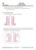
5.4. Case 2 (Customized package pin)
Customized
package pins are shown in the following picture:
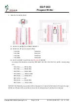
1. You can use the following instruction to define the exclusive package pin:
.writer package
16, 6, 12, 10, 11, 9, 8, 7, 16, 0x00FC, 0x00F1, 0, 0x04
Group
Count
Name
Description
Value
Remark
1
Pin Count
the number of pin
16
2
VDD
VDD pin serial number
6
3
PA0
PA0pin serial number
12
4
PA3
PA3pin serial number
10
5
PA4
PA4 pin serial number
11
6
PA5
PA5 pin serial number
9
7
PA6
PA6 serial number
8
8
PA7
PA7 pin serial number
7
9
GND
GND pin serial number
16
10
Mask1
Package the left pin mask
value
0x00FC
Bypass pin 1, 2.
11
Mask2
Package the right pin mask
value
0x00F1
Bypass pin 15, 14, 13
12
Shift
The blank space IC need to
be shifted
0
The first pin of IC aligns the
upper left first pin of Socket
13
Option
Option Description
0x04
Bit2
:
Write on board
Bit4
:
VDD/VPP swap
Others
:
Reserved


