enabling
innovative
electronics
Ossila Ltd
Copyright © 2009-2015
35
Output characteristic (I-V)
If a constant voltage V
GS
> V
T
is applied to the gate while a varying voltage sweeps
9
the drain, an
output characteristic curve I
DS
(V
DS
) is measured. If this operation is repeated for several V
GS
’s, the
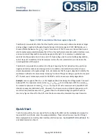
resulting family of output curves constitutes the well-know hallmark of transistor behaviour, see
figure 14.
Figure 14. Output Characteristics (or IV) curves.
The output curves are sometimes referred to as I-V (IV characteristic) curves. In this user manual the
two terms will be used interchangeably.
Note:
It is common practice to acquire at least one I-V curves for V
GS
< V
Th
.
On figure 14, two main transistor
operation regions
are clearly visible. For small V
DS
, the drain
current is linearly dependent on the drain voltage; this constitutes the
linear
or
Ohmic region
. For
large V
DS
, the current tends to saturates (i.e. I
DS
becomes independent of V
DS
) and the transistor is
said to operate in the
saturation region
. A third, important feature of the IV curve in figure 14 is the
so-called
field effect
response of I
DS
, whereby the drain current increase as a larger V
GS
is applied.
A simple visual inspection of figure 13 can help in evaluating the quality of the transistor, contact
resistance and device architecture issues, identify problems with the semiconductor, etc. Refer to
the books mentioned previously [refs 6, 7, and 8] for further information on this.
For the intent and purpose of this manual, the three I-V features detailed above will suffice to
determine the validity of the transistor model. More specifically, the DUT will be considered to
comply with the
standard FET model
if:
1.
For small V
DS
, I
DS
is a linear function of the driving voltage
2.
for larger V
DS,
the current I
DS
saturates
3.
The current I
DS
increase with V
GS
> V
Th
(
field effect
)
For real-world DUT, conditions 1) and 2) may not be strictly satisfied. For example, in presence of
non-Ohmic injection barrier at the drain/semiconductor interface and for small drain voltage, I
DS
9
Sweeping is a common jargon used to describe a measurement where an initial voltage V
start
(or current) is
applied to the DUT, and then gradually increased till a final value V
end
is reached.

