K8DT-PM
4
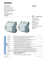
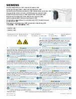
Nomenclature
Front
Note:
Use solid wires, stranded wires, or ferrules to connect to the
terminals.
To maintain the withstand voltage after connecting the
terminals, insert 8 mm of exposed conductor into the terminal.
Indicators
*
This indicator uses the input across L1 and L2 as the internal power
supply. It will not light unless there is an input across L1 and L2.
Setting Knobs
Operation Methods
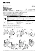
Connections
Input
Wire the input to the L1, L2, and L3 terminals (3-phase, 3-wire).
Make sure the phase sequence is wired correctly. The Unit will not operate normally if the phase
sequence is incorrect.
Outputs
For a relay output, the SPDT contacts are output on terminals 11, 12, and 14. For a transistor
output, the NPN output is on terminals 11 and 14.
Do not use the transistor output for control applications. It is designed only to output a signal when
an error is detected.
Terminal block
(See Note.)
Terminal block
(See Note.)
Power indicator
Output status indicator
Overvoltage knob
(OVER)
Undervoltage knob
(UNDR)
Operating time knob (T)
Alarm indicator
8 mm
8 mm
Solid Wire
8 mm
Stranded Wires
Ferrules
Item
Meaning
Power indicator
(PWR: Green)
Lit when power is being supplied.*
Output status indicator
(OUT: Yellow)
Lights for output (lit for normal operation)
Alarm
indicator
OVER: Red
• Lights for overvoltage error.
When the input exceeds the overvoltage
value, the indicator flashes for the operating
time to indicate the error status.
• Flashes for phase loss.
UNDR: Red
• Lights for undervoltage error.
When the input exceeds the undervoltage
value, the indicator flashes for the operating
time to indicate the error status.
• Flashes for phase loss.
• Flashes for reversed phase error.
Item
Description
Overvoltage knob (OVER)
Used to set from -30% to 30% of the rated
input.
Undervoltage knob
(UNDR)
Used to set from -30% to 30% of the rated
input.
Operating time knob (T)
Used to set the operating time to 0.1 to 30 s.
Voltage input
L1
L2
L3
L3
L2
L1
Load
Contact output
11
14
12
or
11
14
Transistor output