41356801TH Rev.1
118 /
•
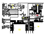
HEAD1 Connector Pin Assignment
(To LED head)
•
HEAD2 Connector Pin Assignment
(To LED head)
1
3
5
7
9
11
13
1
2
3
4
5
6
7
8
9
10
11
12
13
14
C
O
C
O
O
C
O
O
C
O
O
C
O
C
Signal
Description
0VLOGIC
HDCLK-P
0VLOGIC
HDD2-P
HDD3-P
0VLED
HDD0-P
HDD1-P
+3.3V
HDDLD-P
HDSTB1-N
HDSTB2-N
HDSTB3-N
HDSTB4-N
Ground for Logic
Clock
Ground for Logic
Data 2
Data 3
Ground for LED
Data 0
Data 1
+3.3V power supply for LED driving
Load
Strobe 1
Strobe 2
Strobe 3
Strobe 4
PIN NO.
I/O*
2
4
6
8
10
12
14
* O: Out
C: Common
1
3
5
7
9
11
1
2
3
4
5
6
7
8
9
10
11
12
O
O
O
O
O
O
C
C
C
C
C
C
Signal
Description
+3.3V
PIN NO.
I/O*
2
4
6
8
10
12
OVLED
FG
+3.3V power supply for
LED driving
Ground for LED
FG
* O: Out
C: Common
Summary of Contents for OKIPAGE 14
Page 46: ...41356801TH Rev 1 46 Upper cover unit Figure 3 2 Upper cover ...
Page 129: ...41356801TH Rev 1 129 Figure 8 2 Upper cover unit 1 ...
Page 174: ...41356801TH Rev 1 174 5 2 PCB Layout OLEV 11 PCB CN3 CN2 SEN2 ...
Page 175: ...41356801TH Rev 1 175 6 PARTS LIST Figure 6 1 Multi Purpose Feeder 9 5 7 6 4 1 2 3 8 ...
Page 190: ...41356801TH Rev 1 190 CONTROLLER MOTOR DRIVER SEN2 SEN1 OSC PU MOTOR 5 2 PCB Layout TQSB 2 PCB ...
Page 191: ...41356801TH Rev 1 191 Figure 6 1 High Capacity Second Paper Feeder 1 2 4 3 5 6 PARTS LIST ...
Page 194: ...41356801TH Rev 1 194 SECTION1 CABINET CASSETTE ASSEMBLY 5 6 3 2 4 7 8 1 iv iv i i ...


