NXP Semiconductors S32K1 Series Hardware Design Manuallines Download Page 4

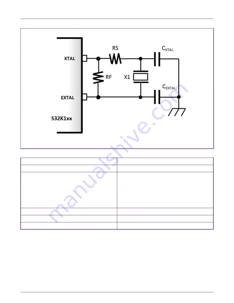
Figure 2. Reference oscillator circuit

Table 2. Components of the oscillator circuit

Symbol

Description

RS

Bias Resistor

RF

Feedback Resistor

• When Low-gain is selected, internal RF will be selected,

and external RF is not required.

• When High-gain is selected, external RF(1M Ohm) need

to be connected for proper operation of crystal. For
external resistor, up to 5% tolerance is allowed.

X1

Quartz Crystal / Ceramic Resonator

C

XTAL

Stabilizing Capacitor

C

EXTAL

Stabilizing Capacitor

The load capacitors are dependent on the specifications of the crystal and on the board capacitance. It is recommended to have
the crystal manufacturer evaluate the crystal on the PCB.

4.2 Suggestions for the PCB layout of oscillator circuit

The crystal oscillator is an analog circuit and must be designed carefully and according to the analog-board layout rules:

• External feedback resistor [Rf] is not needed because it’s already integrated.

NXP Semiconductors

Clock circuitry

Hardware Design Guidelines for S32K1xx Microcontrollers , Rev. 3, December 2018

Application Note

4 / 33

Summary of Contents for S32K1 Series

Page 1: ...of applications including motor control lighting control and body applications Serial communication interfaces such as LPUART LPSPI LPI2C FlexCAN CAN FD FlexIO and so on SHE specification compliant security module Single power supply 2 70 5 5 V with full functional flash program erase read operations Functional safety compliance with ISO26262 with internal watchdog voltage monitors clock monitors ...

Page 2: ...P 144 LQFP 100 LQFP BGA 64 LQFP 48 LQFP QFN 32 LQFP QFN VDDX1 Supply voltage 5 V 3 3 V 10uF 10uF 10uF 10uF 10uF 10uF 0 1uF X7R Ceramic VDDA1 Analog supply voltage 10uF 10uF 10uF 0 1uF X7R Ceramic VREFH1 ADC reference voltage high 0 1uF X7R Ceramic VSS Ground GND VSS VSSA and VREFL must be shorted to GND at package level Table continues on the next page NXP Semiconductors Power supplies Hardware De...

Page 3: ...k FIRC 48 MHz Slow internal reference clock SIRC 8 MHz PLL External oscillator as input source External square wave input clock up to 50 MHz External oscillator clock OSC 4 40 MHz FIRC SIRC are internal and does not have to be considered from the hardware design perspective The external oscillator works with a range from 4 40 MHz It provides an output clock that can be provided to the PLL or used ...

Page 4: ...Stabilizing Capacitor CEXTAL Stabilizing Capacitor The load capacitors are dependent on the specifications of the crystal and on the board capacitance It is recommended to have the crystal manufacturer evaluate the crystal on the PCB 4 2 Suggestions for the PCB layout of oscillator circuit The crystal oscillator is an analog circuit and must be designed carefully and according to the analog board ...

Page 5: ...be connected to VSS x of the S32K1xx with a short trace Never connect the ground guard ring to any other ground signal on the board Also avoid implementing ground loops The main oscillation loop current is flowing between the crystal and the load capacitors This signal path crystal to CEXTAL to CXTAL to crystal should be kept as short as possible and should have a symmetric layout Hence both capac...

Page 6: ...M microcontroller board use a 0 05 20 pin header Samtec FTSH 110 for both debug and trace The signals greyed out are not available on the Cortex M3 or Cortex M4 The 20 pin Cortex Debug D ETM connector support both JTAG and Serial Wire debug protocols When the Serial debug protocol is used the TDO signal can be used for Serial Wire Viewer output for trace capture The connector also provides a 4 bit...

Page 7: ...n smaller 0 05 10 pin connector Samtec FTSH 105 for debug Similar to the 20 pin Cortex Debug D ETM connector both JTAG and Serial Wire debug protocols are supported in the 10 pin version NXP Semiconductors Debug and programing interface Hardware Design Guidelines for S32K1xx Microcontrollers Rev 3 December 2018 Application Note 7 33 ...

Page 8: ...bugger is connected When no debugger is attached this pin is pulled high A debugger connection connects this pin to ground This is used in some development boards that support multiple JTAG con figurations The nSRST connection is optional debugger can reset a Cortex M system via the System Control Block SCB so this connection is often omitted from the top level of microcontroller designs NXP Semic...

Page 9: ...ed example for instruction trace with ETM It can also be used for JTAG SWD connection The 20 pin IDC connector can be connected in parallel with the Mictor connector only one is use at a time NXP Semiconductors Debug and programing interface Hardware Design Guidelines for S32K1xx Microcontrollers Rev 3 December 2018 Application Note 9 33 ...

Page 10: ...ortex processors CortexA8 A9 Cortex R4 or in some multiprocessor systems the trace system might require a wider trace port In such cases some of the other unused pins on the connector will also be used For a typical Cortex M3 or Cortex M4 system the Cortex Debug D ETM connector is recommended NXP Semiconductors Debug and programing interface Hardware Design Guidelines for S32K1xx Microcontrollers ...

Page 11: ...ystem resets and low power modes When RESET_B pin function is disabled it cannot be used as a source for low power mode wake up When the reset pin has been disabled and security has been enabled by means of the FSEC register a mass erase can be performed only by setting both the Mass Erase and System Reset Request fields in the MDM AP register NOTE The reset line has an internal pull up resistor I...

Page 12: ...y introduce some noise to the analog or comparator inputs due to inductance capacitive coupling between the MCU pins The cross talk may be introduced by PCB tracks that run close to each NXP Semiconductors Analog comparator interface Hardware Design Guidelines for S32K1xx Microcontrollers Rev 3 December 2018 Application Note 12 33 ...

Page 13: ...other hand the ground planes also permit high speed digital or analog signals to be transmitted via transmission line microstrip or stripline techniques where controlled impedances are required 7 Communication modules 7 1 LIN interface for LPUART module The Local Interconnect Network LIN is a serial communication protocol designed to support automotive networks As the lowest level of a hierarchica...

Page 14: ...g 1 2 4 8 16 32 64 or 128 idle characters Selectable transmitter output and receiver input polarity Hardware flow control support for request to send RTS and clear to send CTS signals Selectable IrDA 1 4 return to zero inverted RZI format with programmable pulse width Independent FIFO structure for transmit and receive Separate configurable watermark for receive and transmit requests Option for re...

Page 15: ...so no external pull up components are required for the application in a slave node To be used as a master node an external resistor of 1 kΩ in series with a diode must be placed in parallel between VBAT Battery Voltage and the LIN Bus line The fall time from recessive to dominant and the rise time from dominant to recessive is selectable and controlled to guarantee communication quality and reduce...

Page 16: ...ECU from 560 pF up to approximately ten times that value in the slave node CSLAVE so that the total line capacitance is less dependent on the number of slave nodes Tolerance 10 Package Size 0805 Voltage 50 V Mandatory The value of the master node has to be chosen in a way that the LIN specification is fulfilled C2 Capacitor Package Size 0805 Optional Mounting of the optional part only allowed if t...

Page 17: ...N bus lines through a transceiver device The transceiver is capable of driving the large current needed for the CAN bus and has current protection against defective CAN or defective stations A typical CAN system with an S32K1xx microcontroller is shown in Figure 13 on page 17 Figure 13 CAN system The FlexCAN module is a full implementation of the CAN protocol specification the CAN with Flexible Da...

Page 18: ...transceiver circuit Figure 15 CAN physical transceiver circuit with common mode choke NXP Semiconductors Communication modules Hardware Design Guidelines for S32K1xx Microcontrollers Rev 3 December 2018 Application Note 18 33 ...

Page 19: ...he transceiver is optional and the designer might choose not to use it This pin helps stabilize the recessive state of the CAN bus and can be enabled or disabled by software when required LBUS1 Common mode choke A common mode choke on the CANH and CANL lines can help reduce coupled electromagnetic interference and needed to satisfy Automotive EMC requirements This choke together with transient sup...

Page 20: ...ther points in the bus rather than at the two ends Figure 16 d CAN Bus parallel termination 7 2 2 2 Parallel termination with common mode filtering To further enhance signal quality split the terminating resistors at each end in two and place a filter capacitor CSPLIT between the two resistors This filters unwanted high frequency noise from the bus lines and reduces common mode emissions Figure 17...

Page 21: ... AND function The interface is designed to operate up to 100 kbps with maximum bus loading and timing The device is capable of operating at higher baud rates up to a maximum of clock 20 with reduced bus loading The maximum communication length and the number of devices that can be connected are limited by a maximum bus capacitance of 400 pF Figure 18 Connection of I2C bus devices to the I2C bus NX...

Page 22: ...g near and adjacent to a noisy signal the unwanted signals could be coupled in as cross talk It is recommended to keep the signal trace lengths as short as possible Ideally keep the traces under 6 inches Trace length matching to within 2 0 inches on the MII or RMII bus is also recommended Significant differences in the trace lengths can cause data timing issues Minimize the use of vias throughout ...

Page 23: ...eripheral Interface QuadSPI block acts as an interface to external serial flash device It supports SDR and HyperRAM modes upto 4 and 8 bidirectional data lines respectively The QuadSPI supports an A side and a B side The A side of the QuadSPI is connected to the fast pads 80 mA while the B side connects to the 20 mA pads See datasheet for operating values Only one external memory will be supported...

Page 24: ...le HyperRAM on the B side Figure 23 External memory option Single HyperRAM on the B side Single Quad Flash on the B side NXP Semiconductors Quad Serial Peripheral Interface Hardware Design Guidelines for S32K1xx Microcontrollers Rev 3 December 2018 Application Note 24 33 ...

Page 25: ...n the effective output driver strength of 25 33 Ohms and the transmission line characteristic impedance of 50 Ohms one should add the termination resistor close to the output driver to minimize the reflection as shown below Figure 25 Point To Point transmission line Data Signal Routing In order to keep the correct timing for the data transfer from the Microcontroller to the IC Memory the PCB data ...

Page 26: ...nal traces should go with a solid reference plane either GND or VCC Run the clock trace as straight as possible and avoid using serpentine routing Keep a continuous ground in the next layer as reference plane Route the clock trace with controlled impedance Keep the clock signal from disturbance or crosstalk by separating it from other signals by using wider spacing Data bus should be routed with m...

Page 27: ...due to the change in the characteristic impedance Vias also increase the trace length While using differential signals use vias in both traces or compensate the delay in the other trace 10 2 Grounding Grounding techniques apply to both multi layer and single layer PCBs The objective of grounding techniques is to minimize the ground impedance and thus to reduce the potential of the ground loop from...

Page 28: ...and solutions most recommended as applied to CMOS circuits EMI is radio frequency energy that interferes with the operation of an electronic device This radio frequency energy can be produced by the device itself or by other devices nearby Studying EMC for your system allows testing the ability of your system to operate successfully counteracting the effects of unplanned electromagnetic disturbanc...

Page 29: ...propagate from one section of the board to another building up EMI Switching power supplies radiate the energy which can fail the EMI test This is a huge subject and there are many books articles and white papers detailing the theory behind it and the design criteria to combat its effects Every board or system is different as far as EMI EMC and ESD issues are concerned requiring its own solution H...

Page 30: ...ting Ethernet applications and systems The following layer stack ups are recommended for four six and eight layer boards although other options are possible Figure 30 Recommended PCB layer stack up NXP Semiconductors PCB layer stacking Hardware Design Guidelines for S32K1xx Microcontrollers Rev 3 December 2018 Application Note 30 33 ...

Page 31: ...to a safe level per the absolute maximum ratings of the device as long as it is less than the maximum injection current specification For more reference see AN4731 Figure 31 Input protection circuit for I O port 13 References Crystal Oscillator Troubleshooting Guide NXP Semiconductors AN2049 Some Characteristics and Design Notes for Crystal Feedback AN10853 ESD and EMC sensitivity of IC NXP Semico...

Page 32: ...ace on page 11 added 2 02 2018 1 Updated the table Table 1 Power domains and decoupling capacitors on page 2 2 Added the following sections Quad Serial Peripheral Interface on page 23 Injection current on page 31 PCB layer stacking on page 30 Ethernet MAC Interface on page 22 3 12 2018 1 Updated Figure 1 on page 2 2 In Debug and programing interface on page 5 removed the text Usually MCUs do not i...

Page 33: ...NCHIP HITAG I2C BUS ICODE JCOP LIFE VIBES MIFARE MIFARE CLASSIC MIFARE DESFire MIFARE PLUS MIFARE FLEX MANTIS MIFARE ULTRALIGHT MIFARE4MOBILE MIGLO NTAG ROADLINK SMARTLX SMARTMX STARPLUG TOPFET TRENCHMOS UCODE Freescale the Freescale logo AltiVec C 5 CodeTEST CodeWarrior ColdFire ColdFire C Ware the Energy Efficient Solutions logo Kinetis Layerscape MagniV mobileGT PEG PowerQUICC Processor Expert ...

Reviews: