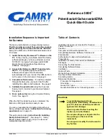
Figure 4. Digital I/O Connector
A1
A2
A3
A4
A5
A6
A7
A8
A9
A10
A11
A12
A13
A14
A15
A16
A17
A18
A19
A20
A21
B1
B2
B3
B4
B5
B6
B7
B8
B9
B10
B11
B12
B13
B14
B15
B16
B17
B18
B19
B20
B21
Reserved
GND
MGT Rx+ 0
MGT Rx– 0
GND
MGT Rx+ 1
MGT Rx– 1
GND
DIO 4
DIO 5
GND
DIO 0
DIO 1
GND
MGT Rx+ 2
MGT Rx– 2
GND
MGT Rx+ 3
MGT Rx– 3
GND
5.0 V
5 V
GND
MGT Tx+ 0
MGT Tx– 0
GND
MGT Tx+ 1
MGT Tx– 1
GND
DIO 6
DIO 7
GND
DIO 2
DIO 3
GND
MGT Tx+ 2
MGT Tx– 2
GND
MGT Tx+ 3
MGT Tx– 3
GND
Reserved
The following table lists the available pins on the DIO connector.
Signal
Type
Direction
MGT Tx± <0..3>
1
Xilinx UltraScale GTH
Output
MGT Rx± <0..3>
1
Xilinx UltraScale GTH
Input
DIO <0..7>
Single-ended
Bidirectional
5.0 V
DC
Output
GND
Ground
—
Notice
The maximum input signal levels are valid only when the module is
powered on. To avoid permanent damage to the PCIe-5774, do not apply a signal to
the device when the module is powered down.
1
MGTs are available only on devices with KU060 FPGAs.
PCIe-5774 Getting Started Guide
|
© National Instruments
|
9