background image

MVME197LE

Single Board Computer

User’s Manual

(MVME197LE/D2)

Summary of Contents for MVME197LE

Page 1: ...MVME197LE Single Board Computer User s Manual MVME197LE D2 ...

Page 2: ...r written permission of Motorola Inc It is possible that this publication may contain reference to or information about Motorola products machines and programs programming or services that are not announced in your country Such references or information must not be construed to mean that Motorola intends to announce such Motorola products programming or services in your country Restricted Rights L...

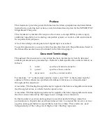
Page 3: ...es the numeric format as follows For example 12 is the decimal number twelve and 12 is the decimal number eighteen Unless otherwise specified all address references are in hexadecimal throughout this document An asterisk following the signal name for signals which are level significant denotes that the signal is true or valid when the signal is low An asterisk following the signal name for signals...

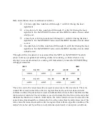
Page 4: ... as shown below Any attempt to use small endian byte ordering will immediately render the MVME197Bug debugger unusable The terms control bit and status bit are used extensively in this document The term control bit is used to describe a bit in a register that can be set and cleared under software control The term true is used to indicate that a bit is in the state that enables the function it cont...

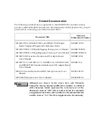
Page 5: ...ars the same number as the manual but has a suffix such as A1 the first supplement to the manual Document Title Motorola Publication Number MVME197LE MVME197DP and MVME197SP Single Board Computers Programmer s Reference Guide MVME197BUG 197Bug Debugging Package User s Manual MVME197BUG 197Bug Diagnostic Firmware User s Manual MVME712M Transition Module and P2 Adapter Board User s Manual MVME712 12...

Page 6: ...ser s Manual SGS Thompson MK48T08 NVRAM TOD Clock Data Sheet The following non Motorola publications may also be of interest and may be obtained from the sources indicated The VMEbus Specification is contained in ANSI IEEE Standard 1014 1987 ANSI IEEE Std 1014 1987 The Institute of Electrical and Electronics Versatile Backplane Bus VMEbus Engineers Incorporated Publication and Sales Department 345...

Page 7: ...ks of their respective holders Copyright Motorola 1993 All Rights Reserved Printed in the United States of America December 1993 WARNING This equipment generates uses and can radiate radio frequency energy and if not installed and used in accordance with the documentation for this product may cause interference to radio communications It has been tested and found to comply with the limits for a Cl...

Page 8: ... not remove equipment covers Only Factory Authorized Service Personnel or other qualified maintenance personnel may remove equipment covers for internal subassembly or component replacement or any internal adjustment Do not replace components with power cable connected Under certain conditions dangerous voltages may exist even with the power cable removed To avoid injuries always disconnect power ...

Page 9: ...on Switches 2 3 Configuration Switch S1 General Information 2 3 Configuration Switch S1 General Purpose Functions S1 1 to S1 8 2 4 Configuration Switch S1 System Controller Enable Function S1 9 2 4 Configuration Switch S6 Serial Port 4 Clock Select S6 1 S6 2 2 5 Connectors 2 5 Installation Instructions 2 5 MVME197LE Module Installation 2 6 System Considerations 2 7 CHAPTER 3 OPERATING INSTRUCTIONS...

Page 10: ...VME197LE Functional Description 4 1 Data Bus Structure 4 1 MC88110 MPU 4 1 BOOT ROM 4 3 FLASH Memory 4 3 Onboard DRAM 4 3 Battery Backup RAM and Clock 4 3 VMEbus Interface 4 4 I O Interfaces 4 4 Serial Port Interface 4 4 Printer Interface 4 5 Ethernet Interface 4 5 SCSI Interface 4 6 SCSI Termination 4 6 Peripheral Resources 4 6 Programmable Tick Timers 4 6 Watchdog Timer 4 7 Software Programmable...

Page 11: ...Figure 2 1 MVME197LE Switches Connectors and LED Indicators Location Diagram 2 2 Figure 4 1 MVME197LE Block Diagram 4 2 Figure A 1 Middle of the Road EIA 232 D Configuration A 5 Figure A 2 Minimum EIA 232 D Connection A 6 ...

Page 12: ...xii ...

Page 13: ...ister Memory Map 3 8 Table 3 6 VMEchip2 Memory Map 3 9 Table 3 7 PCCchip2 Memory Map 3 13 Table 3 8 Printer Memory Map 3 14 Table 3 9 Cirrus Logic CD2401 Serial Port Memory Map 3 15 Table 3 10 82596CA Ethernet LAN Memory Map 3 16 Table 3 11 53C710 SCSI Memory Map 3 17 Table 3 12 MK48T08 BBRAM TOD Clock Memory Map 3 17 Table 3 13 BBRAM Configuration Area Memory Map 3 18 Table 3 14 TOD Clock Memory ...

Page 14: ...xiv ...

Page 15: ...tor P2 A P2 Adapter Board or LCP2 Adapter board routes the signals and grounds from connector P2 to an MVME712 series transition module The MVME197LE supports the MVME712M MVME712A MVME712AM and MVME712B transition boards referred to here as the MVME712X unless separately specified The MVME197LE also supports the MVME712 12 and MVME712 13 referred to as the MVME712 XX unless separately specified T...

Page 16: ...ip the printer port and the BBRAM Battery Backup RAM The VMEchip2 ASIC provides a VMEbus interface The VMEchip2 includes two tick timers a watchdog timer programmable map decoders for the master and slave interfaces and a VMEbus to from the local peripheral bus DMA controller a VMEbus to from the local peripheral bus non DMA programmed access interface a VMEbus interrupter a VMEbus system controll...

Page 17: ...us to VMEbus interface A24 A32 D8 D16 D32 BLT D16 D32 D64 VMEbus interrupter VMEbus interrupt handler Global CSR for inter processor communications DMA for fast local memory VMEbus transfers A16 A24 A32 D16 D32 BLT D16 D32 D64 Specifications The specifications for the MVME197LE are listed in Table 1 1 Table 1 1 MVME197LE Specifications Characteristics Specifications Power requirements Operating te...

Page 18: ...le under test Test software is executed as the module is subjected to ambient temperature variations Case temperatures of critical high power density integrated circuits are monitored to ensure component vendors specifications are not exceeded Characteristics Specifications Physical dimensions PC board Height Width Thickness PC board with connectors and front panel Height Width Thickness Board con...

Page 19: ...es on all external I O ports 2 Cable shields are connected to earth ground via metal shell connectors bonded to a conductive module front panel 3 Conductive chassis rails connected to earth ground This provides the path for connecting shields to earth ground 4 All chassis and MVME197LE front panel attachment screws are properly tightened For minimum RF emissions it is essential that the conditions...

Page 20: ...d with the MVME712 series transition modules Refer to the MVME712 12 MVME712 13 MVME712A MVME712AM and MVME712B Transition Modules and LCP2 Adapter Board User s Manual or the MVME712M Transition Module and P2 Adapter Board User s Manual for more details Software available for the MVME197LE includes SYSTEM V 88 and real time operating systems programming languages and other tools and applications C...

Page 21: ...aterials for storing or reshipping of the equipment Caution Avoid touching areas of integrated circuits Static discharge can damage these components Inspect the equipment for any shipping damage If no damage exists then the module can be prepared for operation according to the following sections of this chapter Hardware Preparation To select the desired configuration and ensure proper operation of...

Page 22: ...Hardware Preparation and Installation 2 2 User s Manual 2 ...

Page 23: ...bus CONNECTOR P1 FAIL LAN RUN A1 B1 C1 A1 B1 C1 DS6 DS5 SCON DS3 VME SCSI ABORT SWITCH S2 RESET SWITCH S3 2 1 20 19 1E1 1A17 1E17 1A1 1E1 2A17 2E17 3A1 3E1 3A17 3E17 O N 1 2 3 4 5 6 7 8 VMEbus CONNECTOR P2 9 O N 1 2 J1 CONFIGURATION SWITCH S6 SERIAL PORT 4 CLOCK SELECT S1 S6 MEZZANINE CONNECTOR J2 MVME197LE Figure 2 1 MVME197LE Switches Connectors and LED Indicators Location Diagram ...

Page 24: ...g Configuration Switch S1 General Information Switch S1 is a bank of nine two way switch segments The following illustration shows the factory configuration of switch S1 The bit values are read as a one when the switch is OFF open and as a zero when the switch is ON closed The default value for switch S1 is shown below Switch S1 System Controller SCON General Purpose Input 7 GPI7 General Purpose I...

Page 25: ...s disabled open Configuration Switch S1 System Controller Enable Function S1 9 The MVME197LE can be the system controller The system controller function is enabled or disabled by configuring selectable switch segment S1 9 When the MVME197LE is the system controller the SCON LED is turned ON The VMEchip2 may be configured as a system controller as illustrated below Factory configuration is with the...

Page 26: ... P2 Connector P1 rows A B C and connector P2 row B provide the VMEbus interconnection Connector P2 rows A and C provide the interconnect to the SCSI bus the serial ports the Ethernet interface and the Centronics printer There is a 249 pin mezzanine connector J2 with the MC88110 bus interface This mezzanine connector is for MVME197LE module expansion There is also a 20 pin general purpose connector...

Page 27: ...ot 1 to correctly initiate the bus grant daisy chain and to have proper operation of the IACK daisy chain driver The MVME197LE is to be installed in the front of the chassis and the MVME712X transition board which has a double wide front panel is to be installed in the rear of the chassis d Carefully slide the MVME197LE module into the card slot Be sure the module is seated properly into the P1 an...

Page 28: ...VME197LE operates as a VMEbus master or as a VMEbus slave it is configured for 32 bits of address and for 32 bits of data A32 D32 However it handles A16 or A24 devices in certain address ranges D8 and or D16 devices in the system must be handled by software Refer to the memory maps in the MVME197LE MVME197DP and MVME197SP Single Board Computers Programmer s Reference Guide The MVME197LE contains s...

Page 29: ...unction as location monitors to allow one MVME197LE processor to broadcast a signal to other MVME197LE processors if any All eight registers are accessible from any local processor as well as from the VMEbus The MVME197LE provides 12 Vdc power to the Ethernet LAN transceiver interface through a 1 amp fuse F2 located on the MVME197LE module If the Ethernet transceiver fails to operate check the fus...

Page 30: ...Hardware Preparation and Installation 2 10 User s Manual 2 ...

Page 31: ...ESET Switch S3 The RESET switch S3 will reset all the onboard devices and drive the SYSRESET signal if the MVME197LE module is the system controller The RESET switch S3 will reset all the onboard devices with the exception of the DCAM and ECDM if the MVME197LE module is not the system controller The VMEchip2 generates the SYSREST signal The BusSwitch combines the local reset and the reset switch t...

Page 32: ...the BRDFAIL signal line is active 2 The green SCON LED DS2 is lit when the VMEchip2 is the VMEbus system controller 3 The green RUN LED DS3 is lit when the MC88110 bus MC pin is low 4 The green LAN LED DS4 lights when the LAN chip is the local peripheral bus master 5 The green VME LED DS5 lights when the board is using the VMEbus or when the board is accessed by the VMEbus 6 The green SCSI LED DS6...

Page 33: ...terface The Processor Bus to Local Peripheral Bus and the Local Peripheral Bus to Processor Bus decoders are programmed in the BusSwitch The Local Peripheral to VMEbus master and VMEbus to Local Peripheral Bus slave decoders are programmed in the VMEchip2 2 Size is approximate 3 Cache inhibit depends on devices in area mapped 4 This area is not decoded If these locations are accessed and the local...

Page 34: ...F02000 FFF02FFF reserved 4KB 4 FFF03000 FFF03FFF reserved 4KB 4 FFF04000 FFF04FFF reserved 4KB 4 FFF05000 FFF05FFF reserved 4KB 4 FFF06000 FFF06FFF reserved 4KB 4 FFF07000 FFF07FFF User defined 4KB 4 FFF08000 FFF3FFFF reserved 224KB 4 FFF40000 FFF400FF VMEchip2 LCSR D32 256B 1 2 3 FFF40100 FFF401FF VMEchip2 GCSR D32 D8 256B 1 2 3 FFF40200 FFF40FFF reserved 3 5KB 4 5 FFF41000 FFF41FFF reserved 4KB ...

Page 35: ...CA must be written as two 16 bit writes upper word first and lower word second 7 DROM BOOT ROM appears at 0 following a local peripheral bus reset The DROM appears at 0 until the DR0 bit is cleared in the PCCchip2 In addition the ROM0 bit in the BusSwitch must be cleared before the DRAM is accessed Detailed I O Memory Maps Tables 3 3 through 3 14 give the detailed memory maps for the BusSwitch reg...

Page 36: ...20 PTR3 PTSR3 PTR4 PTSR4 28 SSAR1 SEAR1 SSAR2 SEAR2 30 SSAR3 SEAR3 SSAR4 SEAR4 38 STR1 STSR1 STR2 STSR2 40 STR3 STSR3 STR4 STSR4 48 PAR1 PAR2 PAR3 PAR4 SAR1 SAR2 SAR3 SAR4 50 BTIMER PADJUST PCOUNT PAL 58 WPPA WPTPA WPPAT 60 ROMCR TCTRL1 TCTRL2 LEVEL MASK ISEL0 ISEL1 68 ABORT CPINT TINT1 TINT2 WPINT PALINT XINT VBASE 70 TCOMP1 TCOUNT1 78 TCOMP2 TCOUNT2 80 GPR1 GPR2 88 GPR3 GPR4 90 XCTAGS 100 XCCR V...

Page 37: ...Memory Maps MVME197LE D2 3 7 3 ...

Page 38: ...2 MEMCON1 03 ECDMID1 04 MEMCON2 05 ECDMID2 06 MEMCON3 07 ECDMID3 08 SYNSTAT0 09 ERSTAT0 0A SYNSTAT1 0B ERSTAT1 0C SYNSTAT2 0D ERSTAT2 0E SYNSTAT3 0F ERSTAT3 10 I2CON0 11 I2STAT0 12 I2CON1 13 I2STAT1 14 I2CON2 15 I2STAT2 16 I2CON3 17 I2STAT3 18 I2DATA0 19 I2ADDR0 1A I2DATA1 1B I2ADDR1 1C I2DATA2 1D I2ADDR2 1E I2DATA3 1F I2ADDR3 D64 D56 D55 D48 D47 D40 D39 D32 D31 D24 D23 D16 D15 D8 D7 D0 ECDM regis...

Page 39: ...OE6 RMWRMOE5 RMWRMOE4 RMWRMOE3 RMWRMOE2 RMWRMOE1 RMWOE5 0F 15 CSRTAIL7 CSRTAIL6 CSRTAIL5 CSRTAIL4 CSRTAIL3 CSRTAIL2 CSRTAIL1 NOT USED 10 16 BWRTTL4 BWRTTL3 BWRTTL2 BWRTTL1 RMWOE4 RMWOE3 RMWOE2 RMWOE1 11 17 SECCLKSL RMWOCKSL BWRITE5 BWRITE4 BWRITE3 BWRITE2 BWRITE1 WRCLKSEL 12 18 NOT USED NOT USED RMW5 RMW4 RMW3 RMW2 RMW1 NOT USED 13 19 RMWTAIL7 RMWTAIL6 RMWTAIL5 RMWTAIL4 RMWTAIL3 RMWTAIL2 RMWTAIL1 ...

Page 40: ...Operating Instructions 3 10 User s Manual 3 ...

Page 41: ...1 14 LOCAL BUS SLAVE ENDING ADDRESS 1 LOCAL BUS SLAVE STARTING ADDRESS 1 18 LOCAL BUS SLAVE ENDING ADDRESS 2 LOCAL BUS SLAVE STARTING ADDRESS 2 1C LOCAL BUS SLAVE ENDING ADDRESS 3 LOCAL BUS SLAVE STARTING ADDRESS 3 20 LOCAL BUS SLAVE ENDING ADDRESS 4 LOCAL BUS SLAVE STARTING ADDRESS 4 24 LOCAL BUS SLAVE ADDRESS TRANSLATION ADDRESS 4 LOCAL BUS SLAVE ADDRESS TRANSLATION SELECT 4 28 LB D16 EN LB WP E...

Page 42: ...Operating Instructions 3 12 User s Manual 3 ...

Page 43: ...us INTERRUPT LEVEL VMEbus INTERRUPT VECTOR DMAC INTERRUPT COUNTER MPU CLR MPU LB EN MPU LB PERR MPU LB OB MPU LB TO DMAC LB EN DMAC LB PERR DMAC LB OB DMAC LB TO DMAC LB ERR DMAC VME ERR DMAC DONE 4C VB TO DMAC TIME OFF DMAC TIME ON VMEbus GLOBAL TIMEOUT VMEbus ACCESS TIMEOUT LOCAL BUS TIMEOUT WATCHDOG TIMEOUT PRESCALER ADJUST 50 TICK TIMER 1 COMPARE 54 TICK TIMER 1 COUNTER 58 TICK TIMER 2 COMPARE...

Page 44: ...Operating Instructions 3 14 User s Manual 3 ...

Page 45: ...27 CLR IRQ 26 CLR IRQ 25 CLR IRQ 24 CLR IRQ 23 CLR IRQ 22 CLR IRQ 21 CLR IRQ 20 CLR IRQ 19 CLR IRQ 18 CLR IRQ 17 CLR IRQ 16 CLR IRQ 15 CLR IRQ 14 CLR IRQ 13 CLR IRQ 12 CLR IRQ 11 CLR IRQ 10 CLR IRQ 9 CLR IRQ 8 78 ACFAIL IRQ LEVEL ABORT IRQ LEVEL SYSFAIL IRQ LEVEL MASTER WRITE POST ERROR IRQ LEVEL PARITY ERROR IRQ LEVEL IRQ1 EDGE SENSITIVE IRQ LEVEL TICK TIMER 2 IRQ LEVEL TICK TIMER 1 IRQ LEVEL 7C ...

Page 46: ...Operating Instructions 3 16 User s Manual 3 ...

Page 47: ...SE CONTROL AND STATUS REGISTER 0 C 6 GENERAL PURPOSE CONTROL AND STATUS REGISTER 1 10 8 GENERAL PURPOSE CONTROL AND STATUS REGISTER 2 14 A GENERAL PURPOSE CONTROL AND STATUS REGISTER 3 18 C GENERAL PURPOSE CONTROL AND STATUS REGISTER 4 1C E GENERAL PURPOSE CONTROL AND STATUS REGISTER 5 D15 D14 D13 D12 D11 D10 D9 D8 D7 D6 D5 D4 D3 D2 D1 D0 NOTES L Local Bus Offset V VMEbus Offset Table 3 6 VMEchip2...

Page 48: ...Operating Instructions 3 18 User s Manual 3 ...

Page 49: ... SCC AVEC SCC RECEIVE IRQ LEVEL 20 SCC MODEM PIACK 24 SCC TRANSMIT PIACK SCC RECEIVE PIACK 28 LAN PAR ERR LAN EXT ERR LAN LTO ERR LAN SCLR LAN PLTY LAN E L LAN INT LAN IEN LAN ICLR LAN IRQ LEVEL LAN SC1 LAN SC2 LAN ERR INT LAN ERR IEN LAN ERR ICLR LAN ERR IRQ LEVEL 2C SCSI PAR ERR SCSI EXT ERR SCSI LTO ERR SCSI SCLR SCSI IRQ SCSI IEN SCSI INT IRQ LEVEL 30 PRTR ACK PLTY PRTR ACK E L PRTR ACK INT PR...

Page 50: ...egister FFF42037 Printer Data Register 16 bits FFF4203A Printer memory map is part of the PCCchip2 refer to PCCchip2 Memory Map BIT 31 30 29 28 27 26 25 24 NAME PLTY E L INT IEN ICLR IL2 IL1 IL0 BIT 23 22 21 20 19 18 17 16 NAME PLTY E L INT IEN ICLR IL2 IL1 IL0 BIT 15 14 13 12 11 10 9 8 NAME PLTY E L INT IEN ICLR IL2 IL1 IL0 BIT 7 6 5 4 3 2 1 0 NAME PLTY E L INT IEN ICLR IL2 IL1 IL0 BIT 31 30 29 2...

Page 51: ...rrupt Status Register high RISRh 88 B R Timer Period Register TPR DA B R W Priority Interrupt level Register 1 PILR1 E3 B R W Priority Interrupt level Register 2 PILR2 E0 B R W Priority Interrupt level Register 3 PILR3 E1 B R W Channel Access Register CAR EE B R W Receive Data Register RDR F8 B R Transmit Data Register TDR F8 B W Local Interrupting Channel Register LICR 26 B R W Local Interrupt Ve...

Page 52: ... the MVME197LE MVME197DP and MVME197SP Single Board Computers Programmer s Reference Guide 2 After reset you must write the System Configuration Pointer to the command registers prior to writing to the CPU Channel Attention register Writes to the System Configuration Pointer must be upper word first lower word second Data Bits Address D31 D16 D15 D0 FFF46000 Upper Command Word Lower Command Word F...

Page 53: ...CL SBDL SIDL SFBR 08 0C SSTAT2 SSTAT1 SSTAT0 DSTAT 0C 10 DSA 10 14 CTEST3 CTEST2 CTEST1 CTEST0 14 18 CTEST7 CTEST6 CTEST5 CTEST4 18 1C TEMP 1C 20 LCRC CTEST8 ISTAT DFIFO 20 24 DCMD DBC 24 28 DNAD 28 2C DSP 2C 30 DSPS 30 34 SCRATCH 34 38 DCNTL DWT DIEN DMODE 38 3C ADDER 3C Address Range Description Size Bytes FFFC0000 FFFC0FFF User Area 4096 FFFC1000 FFFC10FF Networking Area 256 FFFC1100 FFFC16F7 O...

Page 54: ...F8 FFFC1EFB Version 4 FFFC1EFC FFFC1F07 Serial Number 12 FFFC1F08 FFFC1F17 Board ID 16 FFFC1F18 FFFC1F27 PWA 16 FFFC1F28 FFFC1F2B Speed 4 FFFC1F2C FFFC1F33 Ethernet Address 8 FFFC1F34 FFFC1FF6 Reserved 195 FFFC1FF7 Checksum 1 Data Bits Address D7 D6 D5 D4 D3 D2 D1 D0 Function FFFC1FF8 W R S CONTROL FFFC1FF9 ST SECONDS 00 FFFC1FFA x MINUTES 00 FFFC1FFB x x HOUR 00 FFFC1FFC x x x x x DAY 01 FFFC1FFD...

Page 55: ... data structure of the configuration bytes starts at FFFC1EF8 and is as follows The fields are defined as follows 1 Four bytes are reserved for the revision or version of this structure This revision is stored in ASCII format with the first two bytes being the major version numbers and the last two bytes being the minor version numbers For example if the version of a structure is 4 6 this field co...

Page 56: ...iption If the board does not support Ethernet this field is filled with zeros 7 Growth space 195 bytes is reserved This pads the structure to an even 256 bytes Board specific items such as mezzanine board PWA numbers may go here 8 The final one byte of the area is reserved for a checksum as defined in the MVME197BUG 197Bug Debugging Package User s Manual for security and data integrity of the conf...

Page 57: ...pt request registers Local Reset Operation Local reset LRST is a subset of system reset SRST Local reset can be generated five ways by expiration of the watchdog timer by pressing the front panel RESET switch if the system controller function is disabled by asserting a bit in the board control register in the GSCR by SYSRESET or by power up reset Note The GCSR allows a VMEbus master to reset the l...

Page 58: ...Operating Instructions 3 28 User s Manual 3 Any VMEbus access to the MVME197LE while it is in the reset state is ignored If a global bus timer is enabled a bus error is generated ...

Page 59: ... of DRAM 1MB of FLASH memory 128 256KB of BOOT ROM 8KB of static RAM with battery backup a time of day clock with battery backup an Ethernet transceiver interface four serial ports with EIA 232 D interface six tick timers a watchdog timer a SCSI bus interface with DMA Direct Memory Access a Centronics printer port an A16 A24 A32 D8 D16 D32 VMEbus master slave interface and a VMEbus system controll...

Page 60: ...Functional Description 4 2 User s Manual 4 ...

Page 61: ...OR BUS MUX Address RAS CAS Address 32 BusSwitch Mezzanine Port MC88110 ECDM X4 DCAM Data 64 Address Bus Data Bus Data Bus 256 Memory Array 32 64 MB LAN 82596CA VMEbus VMEchip2 SCSI II NCR53710 4 Serial Ports CL CD2401 Flash Memory BOOT ROM PCCchip2 NVRAM RTC Address Bus Data Bus Address 32 Data 32 I2C EEPROM I2 CBus ...

Page 62: ...sfers This memory is controlled by the BusSwitch and the memory size access time and write enable capability can be programmed via the ROM Control Register ROMCR in the BusSwitch The FLASH memory can be accessed from the processor bus only It is not accessible from the local peripheral bus or VMEbus Onboard DRAM The MVME197LE onboard DRAM 2 banks of 32MB memory one optionally installed is sized at...

Page 63: ...ing information I O Interfaces The MVME197LE provides onboard I O for many system applications The I O functions include serial ports a printer port an Ethernet transceiver interface and a SCSI mass storage interface Serial Port Interface The CD2401 serial controller chip SCC is used to implement the four serial ports The serial ports support the standard baud rates 110 to 38 4K baud Serial port 4...

Page 64: ...ace The printer interface is provided by the PCCchip2 Refer to the PCCchip2 chapter in the MVME197LE MVME197DP and MVME197SP Single Board Computers Programmer s Reference Guide for detailed programming information and for drawings of the printer port interface connections Ethernet Interface The 82596CA is used to implement the Ethernet transceiver interface The 82596CA accesses local RAM using DMA...

Page 65: ...systems may include hard and floppy disk drives streaming tape drives and other mass storage devices The SCSI interface is implemented using the NCR 53C710 SCSI I O controller Support functions for the 53C710 are provided by the PCCchip2 Refer to the NCR 53C710 SCSI I O Processor Data Manual and to the PCCchip2 chapter in the MVME197LE MVME197DP and MVME197SP Single Board Computers Programmer s Re...

Page 66: ...e for detailed programming information Processor Bus Timeout The BusSwitch provides a bus timeout circuit for the processor bus When enabled by the BTIMER register in the BusSwitch the timer starts counting when DBB is asserted and if the cycle is not terminated TA TEA or TRTRY asserted before the programmed timeout period TEA is asserted This timer is disabled if the access goes to the local peri...

Page 67: ...The BusSwitch may also generate the non maskable interrupt NMI signal to the MPU from the ABORT push button switch Refer to the BusSwitch PCCchip2 and VMEchip2 chapters in the MVME197LE MVME197DP and MVME197SP Single Board Computers Programmer s Reference Guide for more detailed information ...

Page 68: ...Functional Description 4 10 User s Manual 4 ...

Page 69: ...aking lines were included In many applications these are not needed but since they permit diagnosis of problems they are included in many applications Table A 1 lists the standard DIA 232 D interconnections To interpret this information correctly it is necessary to know that EIA 232 D is intended to connect a terminal to a modem When computers are connected to computers without modems one of them ...

Page 70: ...he modem which indicates that it is permissible to begin transmission of a message When using a modem CTS follows the off to on transition of RTS after a time delay 6 DSR DATA SET READY data set ready is a function supplied by the modem to the terminal to indicate that the modem is ready to transmit data 7 SIG GND SIGNAL GROUND common return line for all signals at the modem interface 8 DCD DATA C...

Page 71: ...n some systems to provide flow control to avoid buffer overflow This is not possible if modems are used It is usually necessary to make CTS high by connecting it to RTS or to some source of 12 volts such as the resistors shown in Figure A 1 It is also frequently jumpered to an MC1488 gate which has its inputs grounded the gate is provided for this purpose Another signal used in many systems is DCD...

Page 72: ...iguration that almost always works If the CTS and DCD signals are not received from the modem the jumpers can be moved to artificially provide the needed signal Figure A 2 shows a way that an EIA 232 D connector can be wired to enable a computer to connect to a basic terminal with only three wires This is because most terminals have a DTR signal that is ON and can be used to pull up the CTS DCD an...

Page 73: ...TIONAL HARDWARE TRANSPARENT MODE RXC LS08 RXD 6850 RTS TXD LS08 RXD 39kΩ 470Ω 12V 12V TXD 20 1 7 2 5 3 4 6 DCD RTS RXD CTS CTS TXC RXC DCD 39kΩ 39kΩ 470Ω 12V 12V 470Ω 470Ω 470Ω 470Ω 12V 1 2 CTS SIG GND DTR DSR LOGIC GND CHASSIS GND 6 8 7 5 SIG GND NC TXD CONNECTOR TO TERMINAL 12V 12V 12V 39kΩ CONNECTOR TO MODEM OR HOST SYSTEM DCD MODULE ...

Page 74: ...ere may be several volts difference in ground potential If pin 1 of the devices are interconnected with a cable several amperes of current could result This not only may be dangerous for the small wires in a typical cable but could result in electrical noise that could cause errors That is the reason that Figure A 1 shows no connection for pin 1 Normally pin 7 should only be connected to the CHASS...

Page 75: ...5 Configuration Switch S1 2 3 2 4 Configuration Switch S6 2 5 Connector P2 2 7 Connectors 1 4 2 5 connectors P1 and P2 2 5 Controls and Indicators 3 1 Cooling Requirements 1 4 D Data Bus Structure 4 1 DCAM I2C Register Memory Map 3 8 DCAM ASIC 1 2 Detailed I O Memory Maps 3 5 diagram s MVME197LE Block 4 2 MVME197LE Switches Connectors and LED Indicators Location 2 2 DROM Download ROM 4 3 E ECDM AS...

Page 76: ... 3 6 CD2401 Serial Port 3 15 DCAM I2C 3 8 ECDM CSR Register 3 7 Ethernet LAN 3 16 Local Devices 3 4 PCCchip2 3 13 printer 3 14 Processor Bus 3 3 SCSI 3 17 VMEchip2 3 9 mezzanine connector 2 5 MK48T08 BBRAM Memory 3 19 MK48T08 BBRAM TOD Clock Memory Map 3 17 module expansion 2 5 MVME197BUG 197Bug Debugging Package User s Manual 1 6 3 20 MVME197Bug debug monitor firmware 197Bug 1 5 MVME197LE Block D...

Page 77: ... ABORT S2 3 1 Configuration S1 2 3 Configuration S6 2 5 front panel 3 1 general purpose functions 2 4 LED 3 2 RESET S3 3 1 serial port 4 clock select 2 5 system controller enable function 2 4 Switches Connectors and LED Indicators Location Diagram 2 2 System Considerations 2 7 system controller 2 4 2 6 SYSTEM V 88 operating system 3 19 T terminal to modem interface A 1 tick timer programmable 4 6 ...

Page 78: ...Index IN 4 User s Manual I N D E X ...

Reviews: