3-20
Theory of Operation:
Transceiver Board
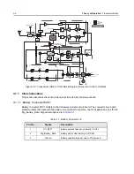
There is a second IC designated U1111 at the output of the radio. This switch routes RF power to the
main antenna or to the accessory GCAII connector on the side of the radio. This switch is controlled
by control line DIG_CNTRL_RMT which connects to pin 13 of the IC. When this signal level is high,
the power is routed to the antenna and when it is low, the power is routed to the accessory
connector.
3.1.3.6 Reverse Power Protection
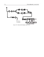
The radio, while in receive mode is constantly monitoring the input power from the antenna. This
power is sensed by the directional coupler and channeled into an RF detector U1106. The matching
network between the coupler and the detector consists of R1107, L1102, C1105 and C1107. Once
the input RF level exceeds a certain limit the detector trips a logic circuit then enables attenuation to
protect the RF front end. This serves as to protect the front end from large signal damage.
3.1.3.7 Transmitter Power Control
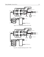
In TX mode, the transmitter Automatic Level Control (ALC) section enables the transmitter and
controls TX power in all modes. Power control is based on a unique dual control loop approach
which utilizes voltage control in one loop and current control in the other. The voltage control loop is
normally used in all transmit modes. The only time the current control loop controls TX power is
during the end of a TX slot in TDMA (F2) mode in the event transmitter saturation is detected.
Several other functions included in the TX ALC section of the radio are RX/TX switching, thermal
cutback of power, current cutback of power, and reverse power detection with a means to disable the
receiver in the event of high reverse power at the antenna port.
3.1.3.7.1 Voltage Control Mode
The heart of the voltage control loop is a logarithmic amplifier based power control IC, U1105. Quad
DAC, U1125, receives the power tuning values via the SPI bus and converts them into a voltage at
"VOUTB." Resistors, R1121 and R1122, form a voltage divider to set the full-scale value of the DAC,
in this case approximately 1.4V. This power set voltage is then fed to the power control IC through
the current cutback op amp, U1130, and then into a lesser-of-two voltage decision circuit, consisting
of U1126 and U1127. This circuit, used exclusively in voltage control mode, provides the important
function of combining the MAKO ramp output with the DAC power set voltage to permit power
leveling since the MAKO DAC max amplitude cannot be controlled during TDMA mode. In all other
TX modes, the MAKO output is a fixed voltage, approximately 1.5V, which is always higher than the
DAC control voltage. The lesser-of-two circuit will then select the smaller input, the set voltage from
U1125, resulting in immediate TX turn on in analog or ASTRO mode. IN TDMA mode, the MAKO line
is a piecewise linear ramp whose timing is in accordance with F2 requirements. At t = 0, the ramp
line is smaller than the TX set voltage so the MAKO ramp will control the TX power level, resulting in
a slower ramping up of the TX power. This continues until the MAKO ramp output reaches the level
of the power tuning DAC (which is always lower than the MAKO ramp maximum) which causes
control of TX power to be turned over to the power tuning DAC.
The output of the selector circuit passes through a 2nd order low pass filter (U1142) and then to the
log amp, U1105. The low pass filter performs the dual function of improving transient ACPR by
transforming a linear ramp with corners into a smooth second order waveform and by acting as a
reconstruction filter for the DAC. The log amp converts RF power fed back from the TX PA into a
current which is summed with the current from the conversion of the setpoint voltage from DAC
U1125. Any imbalance between the RF input level and the level corresponding to the setpoint
voltage is corrected at the VAPC output of the log amp which in turn drives the control voltage input
of the RFPA. The setpoint voltage effectively nulls the error in the loop caused by changes in the RF
level fed back to the log amp. RF from the RFPA is coupled through a directional coupler embedded
in the PC board and passed through a LC equalizer and then to digital attenuator, U1112, which is
used to implement thermal cutback in the event of an over-temperature condition.
Summary of Contents for ASTRO APX 7000
Page 1: ......
Page 4: ...iv Document History Notes ...
Page 24: ...2 4 Radio Power DC Power Routing VOCON Board Notes ...
Page 98: ...3 74 Theory of Operation Global Positioning System GPS ...
Page 163: ...Troubleshooting Charts PA Failure 5 59 ...
Page 164: ...5 60 Troubleshooting Charts PA Failure ...
Page 276: ...7 58 Troubleshooting Tables List of Board and IC Signals Notes ...
Page 318: ...8 42 Schematics Boards Overlays and Parts Lists Transceiver RF Boards VHF 700 800 Notes ...
Page 380: ...8 104 Schematics Boards Overlays and Parts Lists Transceiver RF Boards UHF1 700 800 MHz Notes ...
Page 432: ...8 156 Schematics Boards Overlays and Parts Lists Transceiver RF Boards UHF1 VHF Notes ...
Page 458: ...8 182 Schematics Boards Overlays and Parts Lists Transceiver RF Boards UHF1 UHF2 Notes ...
Page 498: ...8 222 Schematics Boards Overlays and Parts Lists Transceiver RF Boards UHF2 700 800 MHz Notes ...
Page 546: ...8 270 Schematics Boards Overlays and Parts Lists Transceiver RF Boards UHF2 VHF Notes ...
Page 606: ...8 330 Schematics Boards Overlays and Parts Lists VOCON Boards Notes ...
Page 638: ...Glossary 10 Glossary Notes ...
Page 643: ......

