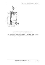
Structure and Assembly/Disassembly of the Machine
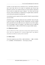
conversion, and then passes the zero adjustment circuit to automatically eliminate the
direct current offset. After the echo signal for beamforming goes through delay
apodization summation, the composite data pass the dynamic aperture compensation
circuit and then the beamforming output is obtained. The circuits have the same
structure, and their characteristics are determined by the applied reception parameters,
such as the delay focusing data and weighting data.
The beamforming circuit is realized in a FPGA, and EP1S10 F672C7 made by ALTERA is
used as the FPGA.
EP1S10F672C7 is one FPGA of the Stratix series made by ALTERA. It features 1M gate,
10,000 LE, 94 blocks of 512bits RAM, 60 blocks of 4Kbits RAM, one block of 512Kbits
RAM, and six DSP blocks (each DSP block can be configured into one 36×36 multiplier,
four 18×18 multipliers or eight 9×9 multipliers). It also supports various 3.3V differential
I/Os and DDR interface. In addition, EP1S10F672C7 also supports the DDR interface.
2.1.1.5Signal processing
There are modules shown as follows: dynamic filter, envelope detection, logarithm compression,
DTGC, odd-even line compensation, AGC, second-time sampling, dynamic range adjustment,
edge enhancement, multiple-focus splicing, and axial smooth filter.
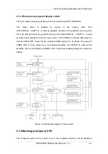
2.1.1.6Cine review
This circuit is realized by means of FPGA
(
ACEX1K100FC484-3
)
, SRAM
(
W24010A-
15
)
and SDRAM
(
HY57V641620HG-T-H
)
. See the figure as follows:
DP-3300/DP-3200
Service Manual
(
V1.1
)
3-9
Summary of Contents for DP-3200
Page 1: ...DP 3300 DP 3200 Digital Ultrasonic Diagnostic Imaging System Service Manual...
Page 2: ......
Page 11: ...DP 3300 DP 3200 Service Manual V1 1 I...
Page 12: ......
Page 16: ......
Page 20: ......
Page 76: ......
Page 81: ...P N 2302 20 34499 V 1 1...

