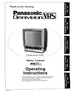
background image

SERVICE MANUAL

Main Section

I

 Specifications

I

 Preparation for Servicing

I

 Adjustment Procedures

I

 Schematic Diagrams

I

 CBA’s

I

 Exploded Views

I

 Parts List

When servicing the deck 
mechanism, refer to MK14 Deck 
Mechanism Section.

Deck Mechanism Part No.: 
N2466FT

20

 ANALOG/DIGITAL            

PURE FLAT COLOR TV/DVD/VCR

CT202MW8

Summary of Contents for CT202MW8

Page 1: ...on for Servicing I Adjustment Procedures I Schematic Diagrams I CBA s I Exploded Views I Parts List When servicing the deck mechanism refer to MK14 Deck Mechanism Section Deck Mechanism Part No N2466F...

Page 2: ...proper service methods may damage the equipment It also is important to understand that these CAUTIONS and NOTICES ARE NOT EXHAUSTIVE Funai could not possibly know evaluate and advice the service trad...

Page 3: ...uctions 1 7 1 How to Initialize the TV DVD VCR 1 8 1 Firmware Renewal Mode 1 9 1 Block Diagrams 1 10 1 Schematic Diagrams CBA s and Test Points 1 11 1 Waveforms 1 12 1 Wiring Diagram 1 13 1 System Con...

Page 4: ...n Unit Nominal Limit 1 Misconvergence Center m m 0 0 4 Corner m m 0 2 5 Side m m 0 1 5 2 Tint Control Range deg 30 23 23 3 Contrast Control Range dB 6 2 4 Brightness 100 White Full Field Contrast Max...

Page 5: ...200 2 Jitter Low R P SP s 0 1 0 2 3 S N Chroma AM R P SP dB 38 33 PM R P SP dB 38 33 4 Wow Fiutter JIS UNWTD R P SP 0 25 0 5 Description Condition Unit Nominal Limit 1 Audio Output Power R P SP W 1 0...

Page 6: ...on Condition Unit Nominal Limit 1 RECEIVED FREQ RANGE 28dBm kHz 150 100 kHz 150 100 2 ATSC DYNAMIC RANGE min max VHF LOW BAND CH 4 VHF HI BAND CH 10 UHF BAND CH 41 dB V dB V dB V 26 114 26 114 28 118...

Page 7: ...en the diode is turned on Do not look directly at the laser beam CAUTION Use of controls and adjustments or doing procedures other than those specified herein may result in hazardous radiation exposur...

Page 8: ...the instrument AC switch in the on position Connect one lead of an ohmmeter to the AC plug prongs tied together and touch the other ohmmeter lead in turn to each tuner antenna input exposed terminal s...

Page 9: ...ected directly to one conductor of the AC power cord and maybe safety serviced without an isolation transformer only if the AC power plug is inserted so that the chassis is connected to the ground sid...

Page 10: ...at sinks oxide metal film resistors fusible resistors etc G Check that replaced wires do not contact sharp edged or pointed parts H When a power cord has been replaced check that 5 6 kg of force in an...

Page 11: ...er cord plug prongs and externally exposed accessible parts RF terminals antenna terminals video and audio input and output terminals microphone jacks earphone jacks etc Measuring Method Power ON Inse...

Page 12: ...l With Hot Air Flat Pack IC Desoldering Machine 1 Prepare the hot air flat pack IC desoldering machine then apply hot air to the Flat Pack IC about 5 to 6 seconds Fig S 1 1 2 Remove the flat pack IC w...

Page 13: ...ead of the flat pack IC upward one by one using a sharp pin or wire to which solder will not adhere iron wire When heating the pins use a fine tip soldering iron or a hot air desoldering machine Fig S...

Page 14: ...rs Fig S 1 6 Note When using a soldering iron care must be taken to ensure that the flat pack IC is not being held by glue When the flat pack IC is removed from the CBA handle it gently because it may...

Page 15: ...ded to remove any static electricity that may be charged on the body 2 Ground for Workbench Be sure to place a conductive sheet or copper plate with proper grounding 1 M on the workbench or other surf...

Page 16: ...ly Preparing 2 1 To eject the tape press the STOP EJECT button on the unit or remote control 2 When you want to record during Service mode press the REC button while depressing SW1211 REC SAFETY SW on...

Page 17: ...P Spring L Locking Tab S Screw CN Connector Unhook Unlock Release Unplug or Desolder e g 2 S 2 two Screws S 2 2 L 2 two Locking Tabs L 2 5 Refer to the following Reference Notes in the Table Step Loc...

Page 18: ...loth human body etc during unpacking or repair work To avoid damage of pickup follow the next procedures 1 Disconnect Connector CN301 on the DVD Main CBA Unit 2 Short the three short lands of the FPC...

Page 19: ...CBA Unit 4 DVD Mechanism 2 Tray Chassis Unit S 8 S 8 Top Shield S 9 S 9 S 9 8 Deck Assembly S 11 S 10 S 12 S 12 S 12 9 Main CBA 10 DTV Module CBA Unit S 5 S 5 S 6 S 6 S 7 S 6 6 Sub CBA 7 Function CBA...

Page 20: ...1 6 4 P7752DC 3 CRT Anode Cap CRT CBA S 4 S 4 S 4 S 4 Fig D3 A DVD Mechanism Fig D4 View for A Short the three short lands by soldering Either of two places FPC Cable...

Page 21: ...TO SPEAKER TO SPEAKER CL2504B SCREEN CL2501B FOCUS CN1802 CL1201 CN1302 CN1301 CL1402 CN1601 CL1401 CL1403 CL2501A CN2571 CN2302 CL2504A CN2301 CN2401 CN2801 CL3801 CN3801 CL3802 CN3802 AC CORD Funct...

Page 22: ...or and short circuit pins 10 and 17 of the microprocessor with a jumper wire How to enter Service mode Service mode 1 Use the service remote control unit 2 Turn the power on Use main power on the TV u...

Page 23: ...ton is pressed YC CONTRAST YC CNT 1 Press 2 button to selcet YC CONTRAST YC CNT display 2 Press CH o p buttons so that the value of YC CONTRAST YC CNT becomes 75 YC COLOR YC COL 1 Press 2 button to se...

Page 24: ...f0 Adjustment Purpose To get correct horizontal position and size of screen image Symptom of Misadjustment Horizontal position and size of screen image may not be properly displayed Note R2583 Sub CBA...

Page 25: ...remote control unit and select COB mode The display will momentarily show COB Adjust the Blue cut off by pressing the CH o p buttons When done with steps 5 6 and 7 the horizontal line should be pure w...

Page 26: ...figure 8 Focus Adjustment Purpose Set the optimum Focus Symptom of Misadjustment If Focus Adjustment is incorrect blurred images are shown on the display Note Focus Control FBT Sub CBA FBT Fly Back Tr...

Page 27: ...ically when 9 button is pressed 4 Input monoscope pattern 5 Press CH o p buttons on the remote control unit so that the monoscope pattern is 90 5 of display size and the circle is round 12 Head Switch...

Page 28: ...rd the bell of the CRT and set it where a uniform red field is obtained 8 Tighten the clamp screw on the Deflection Yoke 14 Convergence Adjustment Purpose To obtain proper convergence of red green and...

Page 29: ...tening the Ring Lock 5 Remove the DY Wedges and slightly tilt the Deflection Yoke horizontally and vertically to obtain the best overall convergence 6 Fix the Deflection Yoke by carefully inserting th...

Page 30: ...rners on TV screen changes from on and off light indication to red by pressing DISPLAY button It is necessary for one or two seconds 6 Press STANDBY ON button to release from Service mode DTV Section...

Page 31: ...it to go to TV mode or press STANDBY ON button on the unit to turn the power off 8 Press SELECT button on the remote control unit to put the TV DVD VCR into DVD mode again 9 Press 1 2 3 4 and DISPLAY...

Page 32: ...MAIN POWER Hi Fi H SW 19 26 2 21 YCA SDA YCA CS DVD AUDIO MUTE 42 5 KEY SWITCH REMOTE SENSOR SW1201 SW1203 SW1206 SW1210 5 5 KEY 1 CN2401 CN2301 CN1104 KEY SWITCH SW2401 SW2408 P ON H2 P ON H2 75 25 1...

Page 33: ...6 REC VIDEO SIGNAL PB VIDEO SIGNAL 57 32 30 QV QH 6dB AMP TO SYSTEM CONTROL SERVO BLOCK DIAGRAM TO TV PROCESS BLOCK DIAGRAM CYLINDER ASSEMBLY RF SW RF SW 59 V ENV V H SW ENV DET ENV DET TP1402 X1401 3...

Page 34: ...UTE SP MUTE 19 19 DVD AUDIO R 17 3 4 17 DVD AUDIO L TO Hi Fi AUDIO BLOCK DIAGRAM 16 9 1 16 DVD AUDIO MUTE 13 13 DTV SPDIF AUDIO OUT R AUDIO OUT L N A IN N A OUT JK2601 WF20 WF8 DTV SPDIF WF7 PB AUDIO...

Page 35: ...54 77 1 39 26 24 27 N A OUT LIM 49 AUDIO OUT L AUDIO OUT R N A IN Hi Fi H SW AUDIO MUTE NORMAL H 40 ST SAP IN TO AUDIO BLOCK DIAGRAM SCL P ON 9V Hi Fi AUDIO R HEAD Hi Fi AUDIO L HEAD CYLINDER ASSEMBL...

Page 36: ...IRCUIT OSD MIX RBG MATRIX BLIGHT DRIVE AMP HV BLANKING TUNER TUNER FILTER TUNING VXCO CF1032 IC1001 IF SIGNAL PROCESS VIF AMP VIDEO DET VCO 4 5MHz FILTER SIF AMP AMP AFT EQ AMP 16 11 13 17 4 7 8 C SYN...

Page 37: ...4 TU SCL 7 7 DTV S SREQ 8 8 DTV S SCLK 9 9 DTV S SIN 10 10 DTV S SOUT 12 12 DTV S RESET DTV S SREQ DTV S SCLK DTV S SOUT DTV S SIN DTV S RESET 189 CN1102 L CH R CH SDA SCL BUS CONT 38 DTV S SREQ 155 D...

Page 38: ...ER ANODE GND V501 CRT GND FOCUS SCREEN JK2501 HEATER 1 1 CL2501B CL2501A CN2571 180V 3 3 11 S F HV FOCUS VR SCREEN VR CN2103 H OUTPUT 1 3 5 4 5 4 3 1 WF13 WF12 WF14 WF10 WF11 RED AMP TP2501 B TP2504 G...

Page 39: ...DVD ON 5V 9 9 EV 3 3V 3 3 EV 1 2V 2 2 EV 1 2V 1 1 EV 1 2V 15 15 PWRCON DVD MAIN CBA UNIT EV 9V DVD ON 5V DVD ON 3 3V EV 3 3V EV 1 2V PWRCON CN1A TO DVD SYSTEM CONTROL SERVO BLOCK DIAGRAM DVD SECTION H...

Page 40: ...OCUS ACTUATOR DRIVE SPINDLE MOTOR DRIVE TRACKING ACTUATOR DRIVE 126 TRAY IN SLD 67 SPDL 66 TRACKING DRIVE 127 FOCUS DRIVE 65 TO DIGITAL SIGNAL PROCESS BLOCK DIAGRAM FS FS TS TS TRAY IN 6 SP 5 SP 1 TRA...

Page 41: ...ERAL I O INTERRUPT CONTROLLER TIMER WATCH DOG TIMER REMOTE CONTROL 32BIT CPU STREAM I F EXTERNAL MEMORY I F SDRAM ECC UMAC 100 115 116 113 114 106 104 105 103 62 DEBUG BCU INST CACHE DATA CACHE 152 15...

Page 42: ...k in the schematic diagram and the parts list Before replacing any of these components read the parts list in this manual carefully The use of substitute replacement parts that do not have the same sa...

Page 43: ...repaired units use only original replacement parts which are listed with their part numbers in the parts list section of the service manual 4 Mode SP REC 5 Voltage indications on the schematics are a...

Page 44: ...1 11 3 Main 1 6 Sensor Schematic Diagram TV VCR Section P7754SCM1...

Page 45: ...1 11 4 P7754SCM2 Main 2 6 Schematic Diagram TV VCR Section...

Page 46: ...1 11 5 P7754SCM3 Main 3 6 Schematic Diagram TV VCR Section...

Page 47: ...1 11 6 Main 4 6 Schematic Diagram TV VCR Section P7754SCM4...

Page 48: ...1 11 7 P7754SCM5 Main 5 6 Junction A Schematic Diagram TV VCR Section...

Page 49: ...at all components in the power supply circuit are not defective before you connect the AC plug to the AC power supply Otherwise it may cause some components in the power supply circuit to fail VOLTAGE...

Page 50: ...1 11 9 P7754SCSUB1 Sub 1 3 Schematic Diagram TV VCR Section...

Page 51: ...1 11 10 Sub 2 3 Schematic Diagram TV VCR Section P7754SCSUB2...

Page 52: ...1 11 11 Sub 3 3 Schematic Diagram TV VCR Section P7754SCSUB3...

Page 53: ...1 11 12 P7754SCCRT P7754SCF Function Junction B Schematic Diagram TV VCR Section CRT Schematic Diagram TV VCR Section...

Page 54: ...1 11 13 P7754SCDT1 DTV Module 1 2 Schematic Diagram TV VCR Section...

Page 55: ...VCR Section CN101 1 0 2 1 9 3 5 2 4 3 4 5 3 4 6 0 7 2 8 8 3 2 9 3 3 10 0 2 11 0 12 3 4 13 0 14 3 2 15 3 2 CN102 1 2 4 9 3 0 4 3 4 5 2 6 6 1 9 7 8 0 9 1 7 10 0 11 0 12 0 13 0 14 2 3 15 2 6 16 2 5 17 0...

Page 56: ...1 11 15 P7754SCD1 DVD Main 1 3 Schematic Diagram DVD Section...

Page 57: ...1 11 16 P7754SCD2 DVD Main 2 3 Schematic Diagram DVD Section...

Page 58: ...1 11 17 P7754SCD3 DVD Main 3 3 Schematic Diagram DVD Section...

Page 59: ...circuit a variable isolation transformer is required NOTE The voltage for parts in hot circuit is measured using hot GND as a common terminal For continued protection against risk of fire replace only...

Page 60: ...voltage for parts in hot circuit is measured using hot GND as a common terminal For continued protection against risk of fire replace only with same type 4 A 125V fuse CAUTION ATTENTION Utiliser un fu...

Page 61: ...1 11 20 B TP2501 BLUE TP1301 TP2504 GND R2583 H f0 Adjustment Sub CBA Top View TV VCR Section BP7750F01021 A...

Page 62: ...1 11 21 WF11 PIN 5 OF CN2571 Q2571 Collector WF10 WF20 H DRIVE TP2503 WF9 PIN 1 OF CN2 WF19 PIN 4 OF CN2 WF18 PIN 6 OF CN2 WF17 PIN 8 OF CN2 Sub CBA Bottom View TV VCR Section BP7750F01021 A...

Page 63: ...1 11 22 WF13 Q2502 Collector WF14 Q2501 Collector WF12 Q2503 Collector CRT CBA Top View TV VCR Section CRT CBA Bottom View TV VCR Section BP7750F01021 B...

Page 64: ...unction B CBA Top View TV VCR Section BP7750F01021 C Function CBA Bottom View TV VCR Section Junction B CBA Bottom View TV VCR Section Junction A CBA Top View TV VCR Section Junction A CBA Bottom View...

Page 65: ...SW 1DIV 0 2V 0 1 s IC1401 Pin 49 1DIV 1V 10ms TP1202 CTL AMP OUT 1DIV 0 25V 20 s IC1401 Pin 32 1DIV 0 5V 20 s TP1401 V OUT Upper WF6 Lower WF1 1DIV 0 2V 2DIV 5V 5ms TP1403 ENV TP1402 RF SW 1DIV 0 5V...

Page 66: ...DATA 14 14 DVD SCLK 15 15 DVD CS 16 16 DVD AUDIO MUTE 17 17 DVD AUDIO L 18 18 P ON 8V 19 19 DVD AUDIO R CN1302 CN2302 1 1 5 7V CTRL 2 2 DVD MAIN POWER 3 3 EXT VIDEO 4 4 GND 5 5 VIDEO 6 6 GND 9 9 DTV Y...

Page 67: ...WRCON EV 3 3V 8 15 9 10 11 12 CN1A PICK UP UNIT CN201 1 2 3 4 5 6 7 8 9 10 11 12 13 14 15 16 17 18 19 20 TS TS FS CD LD FS GND DVD PD GND CD PD PD MONI DVD LD VREF NU GND B P ON 5V CD DVD D A C NU GND...

Page 68: ...00 V 5 00 V CL 0 00 V 0 25 V 0 00 V SB 1 06 V 1 50 V 1 21 V TL 0 66 V 1 05 V 0 91 V FB 1 99 V 2 60 V 2 17 V SF 1 51 V 1 98 V 1 80 V SM 3 20 V 3 75 V 3 40 V AU 0 26 V 0 65 V 0 44 V AL 4 51 V 5 00 V 5 0...

Page 69: ...VE PB CTL 66 C F R STILL STILL FRAME ADVANCE ROLL COMPENSATION DRUM SERVO H A SW 15 ROTA AT The first rise of RF SW after a rise in F AD signal ST T1 BL H H T2 Z 1 SP MODE 1 2 3 4 Acceleration Detecti...

Page 70: ...PB CTL 66 C F R STILL STILL FRAME ADVANCE ROLL COMPENSATION DRUM SERVO H A SW 15 ROTA AT The first rise of RF SW after a rise in F AD signal ST T1 BL H H T2 Z 2 LP EP MODE 1 2 3 4 Acceleration Detect...

Page 71: ...LD REV LD REV LD FWD LD REV LD REV LD REV 0 2S 0 5S CL EJ SS SS AU AU TL Z ON ON PAUSE SLOW AU AL AL AU SF SM POWER OFF STOP PLAY RS FS STILL SLOW PLAY STOP PLAY SB TL SB FB SM SM SF AL AL RS AU AL SS...

Page 72: ...TOP A LD REV FF LD REV LD REV LD FWD LD FWD LD FWD LD FWD LD FWD LD FWD LD FWD REC PAUSE REC REC REW LD REV LD REV LD REV LD REV LD REV LD REV LD REV PAUSE REC or PAUSE STOP EJECT STOP EJECT STOP EJEC...

Page 73: ...Section Tray IN TL221 Sled Drive TP303 Disc Drive TP301 Focus Drive TP304 Tracking Drive TP302 0V 3 3V 0V 1 65V 0V 0V 0V 1 65V 1 65V 1 65V Tray Close Play Play Tray Open Tray Close Disc Rotation Play...

Page 74: ...On Signal 2 at High 29 D REC PB L Delayed Record Playback Control Signal 30 DTV ON H DTV On Signal at High 31 P ON H Power On Signal at High 32 BUS CONT Bus Control 33 REC SAFETY Record Protection Tab...

Page 75: ...Signal 83 DIGITAL AUDIO H Digital Audio Signal 84 P DOWN Power Voltage Down Detector Signal 85 DTV S SREQ DTV Serial Request 86 NU Not Used 87 C FG Capstan Motor Rotation Detection Pulse 88 GND GND AM...

Page 76: ...32A22F LA71205M MPB E LA72670BM MPB E KIA431 AT P M61276FP TF0H M61116FP TF0G AN17812A Note A Anode K Cathode E Emitter C Collector B Base R Reference S Source G Gate D Drain LA78040A 1 IN 2 GND 3 OU...

Page 77: ...Scotch Tape 880 CRT CBA Scotch Tape 880 V501 SP1801 SP801 Function CBA Junction A CBA Junction B CBA L4 TB1 TB9 TL1 2 TL1 2 TB3 TL2 DVD Main CBA Unit TB8 1B1 Main CBA TL5 Sensor CBA TL1 1 TL1 1 TL3 T...

Page 78: ...1 17 2 P7754PEX Packing FRONT S4 S1 X1 Tape X2 X3 S3 S6 S7 S2 Packing Tape...

Page 79: ...L1 SCREW P TIGHT 4X18 BIND HEAD GBJP4180 L2 SCREW TAPPING M4X14 DBT14140 L3 1 SCREW P TIGHT 3X10 BIND HEAD GBHP3100 L3 2 SCREW P TIGHT 3X10 BIND HEAD GBHP3100 L4 SCREW P TIGHT 3X10 BIND HEAD GBJP3100...

Page 80: ...ERAMIC CAP 1608 CH J 22pF 50V CHD1JJ3CH220 C1214 ELECTROLYTIC CAP 47 F 6 3V M H7 CE0KMAVSL470 C1217 CHIP CERAMIC CAP 1608 CH D 10pF 50V CHD1JD3CH100 C1218 CHIP CERAMIC CAP CH J 15pF 50V CHD1JJ3CH150 C...

Page 81: ...2 F 50V M H7 CE1JMAVSL2R2 C1780 ELECTROLYTIC CAP 4 7 F 50V M H7 CE1JMAVSL4R7 C1781 CHIP CERAMIC CAP F Z 1 F 10V CHD1AZ30F105 C1782 ELECTROLYTIC CAP 4 7 F 50V M H7 CE1JMAVSL4R7 C1783 CHIP CERAMIC CAP...

Page 82: ...4C04 WMN6TP NSZAA0TSS015 IC1401 IC Y C A LA71205M MPB E QSZBA0RSY037 Ref No Description Part No IC1601 PHOTOCOUPLER LTV 817C F NPEC0LTV817F IC1682 IC VOLTAGE REGULATOR 5V KIA7805API P NSZBA0SJY041 IC1...

Page 83: ...10W J 680 RRXAJR5Z0681 R1171 CHIP RES 1 10W F 10k RRXAFR5H1002 Ref No Description Part No R1172 CHIP RES 1 10W F 150 RRXAFR5H1500 R1173 CHIP RES 1 10W F 4 7k RRXAFR5H4701 R1174 CARBON RES 1 4W J 390...

Page 84: ...ON RES 1 4W J 180k RCX4JATZ0184 R1609 CARBON RES 1 4W J 10 RCX4JATZ0100 Ref No Description Part No R1610 CARBON RES 1 4W J 1 2k RCX4JATZ0122 R1613 CARBON RES 1 4W J 150 RCX4JATZ0151 R1614 CARBON RES 1...

Page 85: ...W J 47k RRXAJR5Z0473 R1929 CHIP RES 1 10W J 47k RRXAJR5Z0473 SWITCHES SW1201 TACT SWITCH SKQSAB SST0101AL038 SW1202 TACT SWITCH SKQSAB SST0101AL038 SW1203 TACT SWITCH SKQSAB SST0101AL038 SW1206 TACT S...

Page 86: ...470 F 6 3V M CE0KMASDL471 CONNECTORS CN2103 TWG CONNECTOR 19P TWG P19P A1 J3TWA19TG001 CN2301 TWG CONNECTOR 19P TWG P19P A1 J3TWA19TG001 CN2302 TWG CONNECTOR 19P TWG P19P A1 J3TWA19TG001 CN2571 CONNE...

Page 87: ...JATZ0221 R2610 CARBON RES 1 4W J 75 RCX4JATZ0750 R2611 CHIP RES 1 10W J 100 RRXAJR5Z0101 R2613 CARBON RES 1 4W J 1 RCX4JATZ01R0 R2617 CARBON RES 1 4W J 390 RCX4JATZ0391 R2618 CARBON RES 1 4W J 390 RCX...

Page 88: ...JATZ0152 MISCELLANEOUS JK2501 CRT SOCKET ISMP02S JSCC220PK009 Ref No Description Part No FUNCTION CBA MPS C Consists of the following CONNECTORS CN2401 BOARD CONNECTOR 07P PB FREE 127301107K2 JCTWA07T...

Page 89: ...erein without the obligation to notify any person or organization of such changes with the design is a registered trademark of Funai Electric Co Ltd and may not be used in any way without the express...

Reviews: