25
LTC3729
sn3729 3729fas
APPLICATIO S I FOR ATIO
W
U
U
U
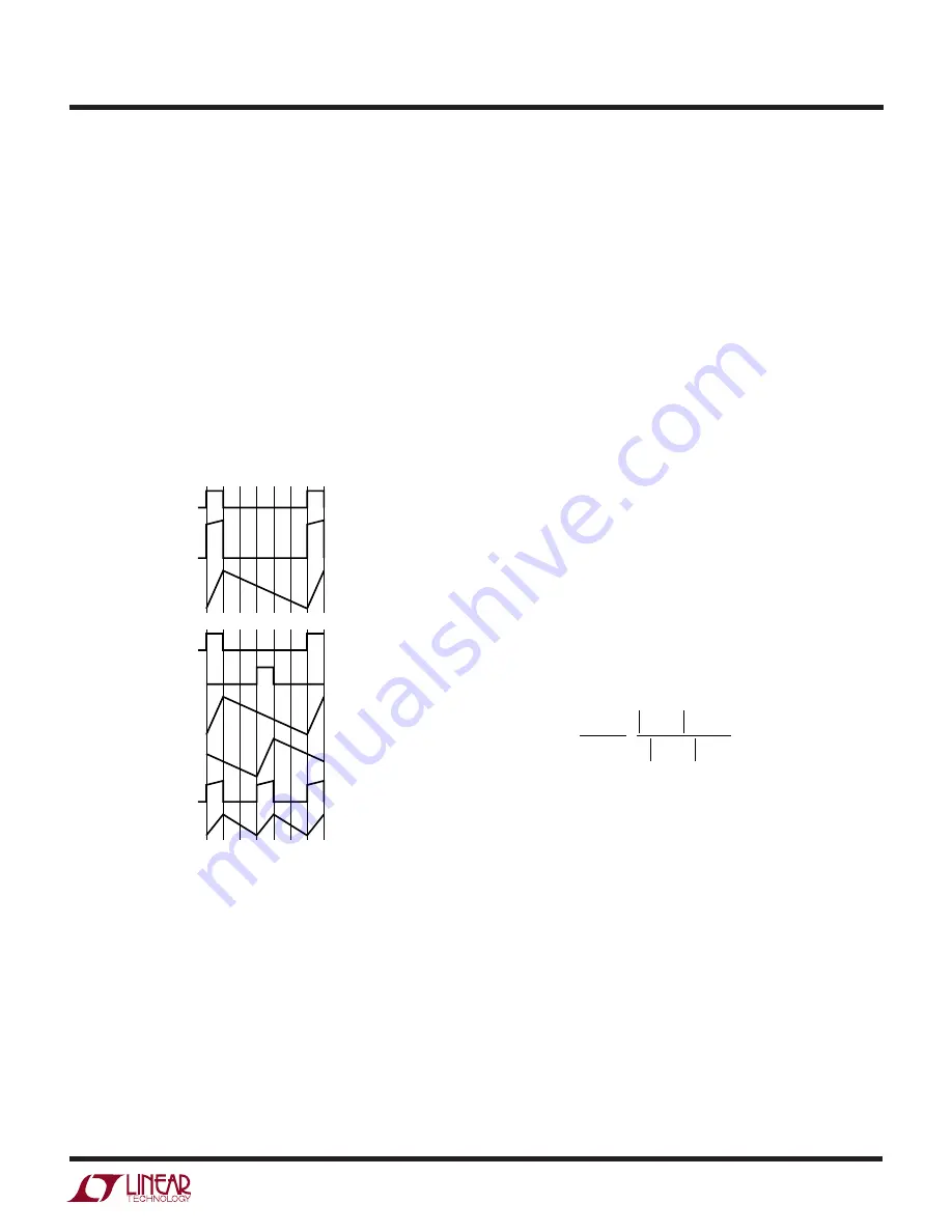
Simplified Visual Explanation of How a 2-Phase
Controller Reduces Both Input and Output RMS Ripple
Current
A multiphase power supply significantly reduces the
amount of ripple current in both the input and output
capacitors. The RMS input ripple current is divided by, and
the effective ripple frequency is multiplied up by the
number of phases used (assuming that the input voltage
is greater than the number of phases used times the output
voltage). The output ripple amplitude is also reduced by,
and the effective ripple frequency is increased by the
number of phases used. Figure 10 graphically illustrates
the principle.
Figure 10. Single and PolyPhase Current Waveforms
I
CIN
SW V
I
COUT
I
CIN
SW1 V
DUAL PHASE
SINGLE PHASE
SW2 V
I
COUT
RIPPLE
3729
F10
I
L1
I
L2
The worst-case RMS ripple current for a single stage
design peaks at twice the value of the output voltage . The
worst-case RMS ripple current for a two stage design
results in peaks at 1/4 and 3/4 of input voltage. When the
RMS current is calculated, higher effective duty factor
results and the peak current levels are divided as long as
the currents in each stage are balanced. Refer to Applica-
tion Note 19 for a detailed description of how to calculate
RMS current for the single stage switching regulator.
Figures 3 and 4 help to illustrate how the input and output
currents are reduced by using an additional phase. The
input current peaks drop in half and the frequency is
doubled for a 2-phase converter. The input capacity
requirement is reduced theoretically by a factor of four!
A ceramic input capacitor with its unbeatably low ESR
characteristic can be used.
Figure 4 illustrates the RMS input current drawn from the
input capacitance versus the duty cycle as determined by
the ratio of input and output voltage. The peak input RMS
current level of the single phase system is reduced by 50%
in a 2-phase solution due to the current splitting between
the two stages.
An interesting result of the multi-phase solution is that the
V
IN
which produces worst-case ripple current for the input
capacitor, V
OUT
= V
IN
/2, in the single phase design pro-
duces zero input current ripple in the 2-phase design.
The output ripple current is reduced significantly when
compared to the single phase solution using the same
inductance value because the V
OUT
/L discharge current
term from the stage(s) that has its bottom MOSFET on
subtracts current from the (V
IN
- V
OUT
)/L charging current
resulting from the stage which has its top MOSFET on. The
output ripple current is:
I
V
fL
D
D
D
RIPPLE
OUT
=
−
−
( )
−
+
2
1 2 1
1 2
1
where D is duty factor.
The input and output ripple frequency is increased by the
number of stages used, reducing the output capacity
requirements. When V
IN
is approximately equal to NV
OUT
as illustrated in Figures 3 and 4, very low input and output
ripple currents result.
Again, the interesting result of 2-phase operation results
in no output ripple at V
OUT
= V
IN
/2. The addition of more
phases by phase locking additional controllers always
results in no net input or output ripple at V
OUT
/V
IN
ratios
equal to the number of stages implemented. Designing a
system with a multiple of stages close to the V
OUT
/V
IN
ratio
will significantly reduce the ripple voltage at the input and
outputs and thereby improve efficiency, physical size, and
heat generation of the overall switching power supply.


