background image


C

OPYRIGHT

©


This document is a copyright of the original manufacturer, 2002.    The original manufacturer reserves 
the rights to make improvement and/or modification to the product described in this manual at any 
time without further notice.  This manual may not, in whole or in part, be photocopied, reproduced, 

transcribed, translated, or transmitted in whatever form without the written consent of the 
manufacturer, except for copies retained by the purchaser for backup purposes.  All rights are 

reserved. 


TRADEMARKS                                                                                                                           


The following are trademarks or registered trademarks of their respective companies: IBM, Intel, AMD, 
Cyrix, NS, Award, AMI, Microsoft, Windows, Windows NT, Novell, SCO, PC/104, PICMG, ALI, UMC, VIA, 

S3, Realtek, SMC and Winbond. Products mentioned in this manual are mentioned for identification 
purposes only.  All names of products or services appearing in this manual are the trademarks or 

registered trademarks of their respective organizations and companies.   
 

 Copyright 2003


                                                                                                                                                                    Version:  1.0       

Date: 2003/07/11 

Summary of Contents for EM-568 Series

Page 1: ...EM 568 Series EBX SBC with VIA CPU VGA LCD LVDS Audio Ethernet CF PC 104 and PCI expansion USER S MANUAL...

Page 2: ...ufacturer except for copies retained by the purchaser for backup purposes All rights are reserved TRADEMARKS The following are trademarks or registered trademarks of their respective companies IBM Int...

Page 3: ...AWARD BIOS 27 3 2 CMOS SETUP UTILITY 28 3 3 STANDARD CMOS SETUP 30 3 4 BIOS FEATURES SETUP 33 3 5 CHIPSET FEATURES SETUP 35 3 6 INTEGRATED PERIPHERALS 38 3 7 POWER MANAGEMENT SETUP 40 3 8 PNP PCI CONF...

Page 4: ......

Page 5: ...e is EIDE and the other one is CF II EIDE supports four IDE devices EM 568 offers 2 IDE box header to fulfill flexible hard disk placement in system design Regarding to CF II socket system can further...

Page 6: ...04 connector ISA Expansion Bus PCI slot Serial Port FOUR Chip VT686B Winbond W83877TF COM Setting COM 1 3 4 is RS 232 COM 2 is RS 232 422 485 setting by jumper COM Power 4 COMs pin 9 all with 5V 12V s...

Page 7: ...Key z FDC cable x 1 pc 0800100340002 34P TO 34P P4 with Key z IDE cable x 1 pc 0800100400004 ATA100 40P 80 Impendence P20 with Key z USB Y cable x 1 pc 080019F100001 2 5P 2 54mm with P9 z VGA cable x...

Page 8: ...Chapter 1 Introduction 4 User s Manual 1 5 Board Layout...

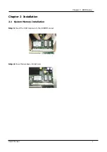
Page 9: ...Chapter 3 BIOS Setup 5 User s Manual Chapter 2 Installation 2 1 System Memory Installation Step 1 Insert the RAM module into the SODIMM socket Step 2 Press Module down till clip hold...

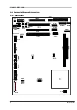
Page 10: ...BA1 USBA2 CPU1 1 1 A B D C 2 1 10 9 DIOA1 2 1 10 9 1 LCD1 2 49 50 LVDSD1 1 20 1 5 LVDSC1 1 2 29 30 VGAB1 11 12 2 1 VLCD1 1 3 2 1 8 7 IRDA1 1 5 LPTA1 1 2 26 25 2 8 1 7 PKMB1 FDCA1 IDEA1 COMD1 1 7 PS7M1...

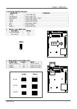
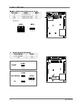
Page 11: ...oltage SBVA1 Select AT ATX Power SCF1 Master Slave Select JFA1 Factory Setting SLCDA1 Select Panel Type z CMOS1 Clear CMOS Data Description CMOS1 Normal Default 1 2 Clear CMOS 2 3 z SC2T1 SC2T2 Select...

Page 12: ...z VLCD1 Select Panel Voltage Panel Voltage VLCD1 3 3V Default 1 2 5V 2 3 Pin 9 Type SRIV1 SRIV2 RI 1 5 2 6 3 7 4 8 1 2 5V 5 9 6 10 7 11 8 12 1 2 12V 5 9 6 10 7 11 8 12 2 3 VLCD1 3 3V Default VLCD1 5V...

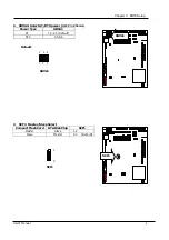
Page 13: ...BVA1 Select AT ATX power 2x3 Pin 2 54mm Power Type SBVA1 AT 1 3 2 4 Default ATX 3 5 4 6 z SCF1 Master Slave Select Compact Flash Card ATA Disk Chip SCF1 Master Slave 1 2 Slave Master 2 3 Default Defau...

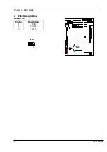
Page 14: ...Chapter 3 BIOS Setup 10 User s Manual z JFA1 Factory Setting Defaut 1 2 Pin No Description 1 3VSB 2 Pin A14 3 GNT1 JFA1 1 3 JFA1...

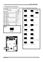
Page 15: ...1024 x 768 TFT 1pixel Clk at 65MHZ 7 8 640 x 480 TFT 1 2 3 4 5 6 800 x 600 TFT 3 4 5 6 1024 x 768 TFT 1 2 5 6 1280 x 1024 TFT 5 6 1400 x 1050 TFT 2pixel Clk at 54MHZ 1 2 3 4 800 x 600 DSTN 3 4 1024 x...

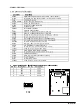
Page 16: ...ctor USBA1 USB Port 1 2 Connector 2 5 Pin 2 54mm USBA2 USB Port 3 4 Connector 2 5 Pin 2 54mm PKMB1 PS 2 Keyboard Mouse Connector 2 4 Header 2 54mm VGAB1 External VGA Connector 12 Pin Header IDEA1 IDE...

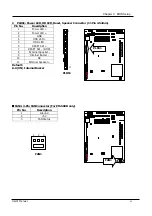
Page 17: ...escription 1 Power LED 2 Power LED 3 GND 4 HDD LED 5 HDD LED 6 RESET SW 7 RESET SW GND 8 External Speaker 9 Internal Buzzer 10 NC 11 External Speaker z z z zFAN1 3 Pin FAN Connector For EM 568B only P...

Page 18: ...D2 12V LA19 IRQ15 8 SD1 0 WS LA18 IRQ14 9 SD0 12V LA17 DACK0 10 IOCHRDY NC MEMR DRQ0 11 AEN SMEMW MEMW DACK5 12 SA19 SMEMR SD8 DRQ5 13 SA18 IOW SD9 DACK6 14 SA17 IOR SD10 DRQ6 15 SA16 DACK3 SD11 DACK7...

Page 19: ...z zLANH1 RJ 45 180 LAN Connector Description Pin No Fast E Net 1 TX 2 TX 3 RX 4 T45 5 T45 6 RX 7 T78 8 T78 z z z zLEDD1 2x2 Pin Lan Link Active LED Pin No Signal Pin No Signal 1 3VSB 2 LINK LED 3 3VS...

Page 20: ...No Description 1 GND 2 5V 3 12V 4 ENAVEE 5 Bright Regular pin 5 bright output is 1 8V But output can be adjusted by below software tools E568LAWD EXE for output 0 3 3V Brightness Adjust Operation Powe...

Page 21: ...W 11 A8 36 WE 12 A7 37 READY 13 CFVCC3 38 CFVCC3 14 A6 39 CSEL 15 A5 40 VS2 16 A4 41 RESET 17 A3 42 WAIT 18 A2 43 INPACK 19 A1 44 REG 20 A0 45 DASP 21 DATA0 46 DIAG 22 DATA1 47 DATA8 23 DATA2 48 DATA9...

Page 22: ...No Description 1 USB_VCC 2 USB_VCC 3 USBD2 4 USBD3 5 USBD2 6 USBD3 7 Ground 8 Ground 9 KEY 10 USB Ground 4 z z z zPKMB1 PS 2 Keyboard Mouse Connector 2x4 Header 2 54mm Pin No Description Pin No Descri...

Page 23: ...r Pin No Description Pin No Description 1 Reset 2 Ground 3 Data 7 4 Data 8 5 Data 6 6 Data 9 7 Data 5 8 Data 10 9 Data 4 10 Data 11 11 Data 3 12 Data 12 13 Data 2 14 Data 13 15 Data 1 16 Data 14 17 Da...

Page 24: ...14 17 Data 0 18 Data 15 19 Ground 20 Key 21 DMA REQ 22 Ground 23 IOW 24 Ground 25 IOR 26 Ground 27 IOCHRDY 28 Ground 29 DMA ACK 30 Ground 31 Interrupt 32 NC 33 SA1 34 PD80P 35 SA0 36 SA2 37 HDC CS0 38...

Page 25: ...Density Select 3 Ground 4 KEY 5 Ground 6 DS1 7 Ground 8 Index 9 Ground 10 Motor Enable A 11 Ground 12 Drive Select B 13 Ground 14 Drive Select A 15 Ground 16 Motor Enable B 17 Ground 18 Direction 19...

Page 26: ...Ground 15 Data6 16 Ground 17 Data7 18 Ground 19 Acknowledge 20 Ground 21 Busy 22 Ground 23 Paper Empty 24 Ground 25 Printer Select 26 KEY z z z zLVDSC1 LVDS Panel Connector 2x15P 1 0mm SMT Pin No Desc...

Page 27: ...IN1 4 NRTS1 5 NSOUT1 6 NCTS1 7 NDTR1 8 CA D9 9 GND 10 NC 11 COM2_1 12 NDSR2 13 COM2_2 14 NRTS2 15 COM2_3 16 NCTS2 17 COM2_4 18 CB P9 19 GND 20 NC 21 NDCD3 22 NDSR3 23 NSIN3 24 NRTS3 25 NSOUT3 26 NCTS3...

Page 28: ...GND 12 GND 13 P0 14 P1 15 P2 16 P3 17 P4 18 P5 19 P6 20 P7 21 P8 22 P9 23 P10 24 P11 25 P12 26 P13 27 P14 28 P15 29 GND 30 P16 31 P17 32 P18 33 P19 34 P20 35 P21 36 P22 37 P23 38 GND 39 P24 40 P25 41...

Page 29: ...5 User s Manual z z z zPS4W1 4 Pin Power Connector WAFER 4P 2 00mm Pin No Description 1 GND 2 5V 3 GND 4 12V z z z zATXC1 For ATX Function Pin No Description 1 GND 2 5V STANDBY 3 GND 4 PSON PS4W1 1 4...

Page 30: ...ption 1 PANSW 2 GND z z z zLVDSD1 LVDS CONNECTOR 20Pin 1 27mm Pitch Optional Pin No Description 1 FVCC 2 FVCC 3 GND 4 GND 5 RXIN0 6 RXIN0 7 GND 8 RXIN1 9 RXIN1 10 GND 11 RXIN2 12 RXIN2 13 GND 14 RXCLK...

Page 31: ...s The POST routines perform various diagnostic checks while initializing the board hardware If the routines encounter an error during the tests the error will be reported in one of two ways a series o...

Page 32: ...d Chipset Features Set Supervisor Password f Integrated Peripherals Set User Password f Power Management Setup Save Exit Setup f PnP PCI Configurations Exit Without Saving Esc Quit Select Item F10 Sav...

Page 33: ...t Setup Use this Menu to specify your settings for power management PnP PCI Configurations This entry appears if your system supports PnP PCI PC Health Status This entry shows your PC health status If...

Page 34: ...Drive B None Halt On All But Disk Key Base Memory 640K Extended Memory 252928K Total Memory 253952K Move Enter Select PU PD Value F10 Save ESC Exit F1 General Help F5 Previous Values F7 Optimized Def...

Page 35: ...one If the controller of HDD interface is CD ROM the selection shall be None Here is a brief explanation of drive specifications z Access Mode The settings are Auto Normal Large and LBA z Cylinder Num...

Page 36: ...S detects a non fatal error the system will not be stopped and you will be prompted All errors The system boot will be stopped for any error that may be detected All But Keyboard The system boot will...

Page 37: ...llow you to choose the VIRUS warning feature for IDE Hard Disk boot sector protection If this function is enabled and someone attempt to write data into this area BIOS will show a warning message on s...

Page 38: ...protect the Setup Utility settings from being tampered with Select System if you want to use password feature every time the system boots up The default setting is Setup You can create your password b...

Page 39: ...abled Enabled Disabled Enabled Disabled Disabled Move Enter Select PU PD Value F10 Save Esc Exit F1 General Help F5 Previous Values F7 Optimized Defaults Spread Spectrum When the system clock generato...

Page 40: ...to for avoiding any error in your system The default setting is Auto AGP Driving Value This item allows you to adjust the AGP driving force Panel Type Please select the type of panel you are incorpora...

Page 41: ...ates are used allowing for greater stability but check with your motherboard manufacturer to see if they have already implemented a Master latency of zero in which case the lowest writing here of 1 wi...

Page 42: ...nabled 3F8 IRQ4 2F8 IRQ3 Normal Half 378 IRQ7 SPP 3 Epp1 9 Disabled IRQ10 Disabled IRQ11 Enabled Move Enter Select PU PD Value F10 Save Esc Exit F1 General Help F5 Previous Values F7 Optimized Default...

Page 43: ...lows you to select the is half full duplex function The default setting is Half Onboard Parallel Port This item allows you to determine onboard parallel port controller I O address setting The setting...

Page 44: ...Date of Month 0 Resume Time hh mm ss 0 48 2 PwrOn After AC Power Loss On Move Enter Select PU PD Value F10 Save Esc Exit F1 General Help F5 Previous Values F7 Optimized Defaults ACPI Function This it...

Page 45: ...ation ports and write blank to the video buffer Blank Screen This option only writes blanks to the video buffer DPMS Initial display power management signaling Suspend Mode Power saving by suspends mo...

Page 46: ...NT Pin 4 Assignment Auto Select Yes if you are using a Plug and Play capable operating system Select No if you need the BIOS to configure non boot devices Move Enter Select PU PD ValueF10 Save Esc Exi...

Page 47: ...ion PCI ISA PnP for devices compliant with the Plug and Play standard whether designed for PCI or ISA bus architecture DMA Resources The sub menu can let you control the DMA resource Item Help Menu Le...

Page 48: ...hoenix Award BIOS CMOS Setup Utility PC Health Status CPU Temperature 38 100 Item Help System Temperature 27 80 Menu Level f FAN1 0 RPM Vcore 1 17 V 2 5V 2 47 V 3 3V 3 25 V 5V 4 92 V Move Enter Select...

Page 49: ...t are factory settings for optimal performance system operations Phoenix Award BIOS CMOS Setup Utility fStandard CMOS Features fAdvanced BIOS Features fAdvanced Chipset Features fIntegrated Peripheral...

Page 50: ...in BIOS FEATURES SETUP will determine when entering the password will be required Phoenix Award BIOS CMOS Setup Utility fStandard CMOS Features fAdvanced BIOS Features fAdvanced Chipset Features fInte...

Page 51: ...he booting process Phoenix Award BIOS CMOS Setup Utility fStandard CMOS Features fAdvanced BIOS Features fAdvanced Chipset Features fIntegrated Peripherals fPower Management fPnP PCI Configure fPC Hea...

Page 52: ...anging old ones Phoenix Award BIOS CMOS Setup Utility fStandard CMOS Features fAdvanced BIOS Features fAdvanced Chipset Features fIntegrated Peripherals fPower Management fPnP PCI Configure fPC Health...

Page 53: ...in the package Please follow the instructions set forth on the screen carefully 1 Find the directory for your O S accordingly 2 Always read the README TXT before installation 3 Run the EXE and follow...

Page 54: ...O443 The system will reboot automatically according to the time out you set Enable Disable C DOS DEBUG C DOS DEBUG O 443 0 F O 441 0 F EX 2 For assemble Language Enable MOV DX 443H OUT DX AL Disable M...

Page 55: ...turned at the customer expense 5 The following conditions are excluded from this warranty A Improper or inadequate maintenance by the customer B Unauthorized modification or misuse C Operation outside...

Page 56: ...press Others Item Model Name Serial Number Configuration Item Problem Code Failure Status Problem Code 01 D O A 02 Second Time R M A 03 CMOS Data Lost 04 FDC Fail 05 HDC Fail 06 Bad Slot 07 BIOS Probl...

Reviews: