DV-5050M/5900M/DVF-J6050/J6050-G
18
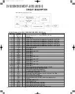
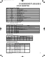
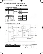
CIRCUIT DESCRIPTION
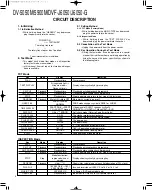
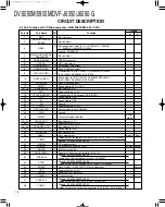
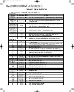
Port No.
Port Name
I/O
Function
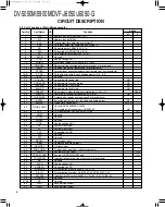
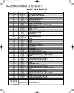
External OSD Interface
1~5
OSDC(0~4)
I
Multiplexed chroma signal is input on this bus. ( Connected to ground.)
156~160
OSDC(5~9)
6
OSDSEL
-
External OSD select input. (Connected to ground.)
144~153
OSDY(0~9)
-
External OSD luma input. (Connected to ground.)
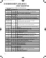
Test outputs(Not shown on Block diagram)
7~10
TEST(03~06)
O
Test outputs. These pins should be left unconnected for normal operation.
13~15
TEST(00~02)
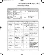
Test inputs(Not shown on Block diagram)
19
TESTB
I
Active low test input. This pin should be tied to VDD for normal operation.
69,70,143
TEST (0~2)
I
Active high test inputs. This pin should all be tied to VSS for normal operation.
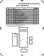
Power Supply Connections(Not shown on Block diagram
11,28,40,49,59,60,81,
87,93,99,101,107,
VDD
-
Digital power connections. Connect to the d3.3 volt power
113,119,121,127,
supply and decouple to the digital ground plane.
131,135,141,154
12,29,41,50,79,80,82,
88,94,100,102,108,
VSS
-
Digital ground connections. Connect to the digital ground plane.
114,120,122,128,
132,136,142,155
72
ISINK
-
Analog current sink return for the video DAC circuits. Connect to the analog
ground plane.
68
AVDD
-
Analog power connections for the clock PLL circuits.
74
AVDD
-
Analog power connections for the video DAC circuits.
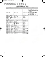
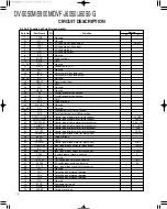
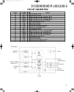
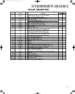
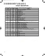
Control Signals
16
SDA
I
I
2
C compatible serial control bus data.
17
SCL
I/O I
2
C compatible serial control bus clock.
18,20
MODE(0,1)
-
I
2
C operating MODE( 0,1).
21~23
ADDR(0~2)
-
The setting of ADDR(0~2) allow the I
2
C address of the device to be
programmed to prevent conflict with the other I
2
C devices in the system.
24
I
2
CCLK
I
Clock input for the internal I2C circuit.
25
RESETB
I
Reset. When this input is set low it will reset all internal registers
to the default states.
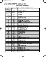
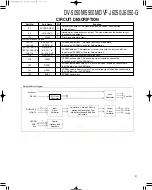
I
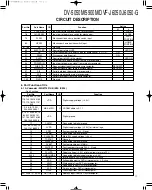
Master clock input.
-
When this pin is set low the FL12220 will be in normal enhancement mode.
I
10-bit non-multiplexed Cb or multiplexed Cb/ Cr signal input bus.
I
10-bit non-multiplexed Cr signal input bus.
I
10bit luminance or multiplexed Y/Cb/Cr signal input bus.
I
Horizontal input blanking signal.
I
Vertical input blanking signal.
I
Odd/Even field designator input.
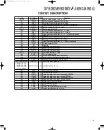
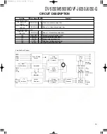
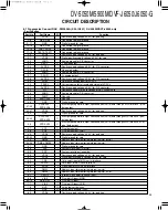
Analog Output Signals
71
R/Cr-ANA
O
Analog output.
73
G/Y-ANA
O
Analog output.
75
B/Cb-ANA
O
Analog output.
76
COMP
-
Compensation for video DACs. Should be connected to analog
groundvia a capacitor.
77
RSET
-
Current setting resistor for video DACs.
78
VREF
-
Voltage reference for video DACs.
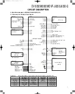
6-4 Digital Video Enhancer : FL12220 (X35, IC703) DV-5900M only
• Port Function
www. xiaoyu163. com
QQ 376315150
9
9
2
8
9
4
2
9
8
TEL 13942296513
9
9
2
8
9
4
2
9
8
0
5
1
5
1
3
6
7
3
Q
Q
TEL 13942296513 QQ 376315150 892498299
TEL 13942296513 QQ 376315150 892498299

