DV-5050M/5900M/DVF-J6050/J6050-G
23
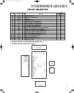
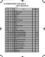
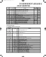
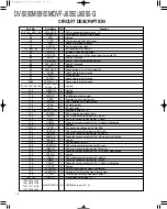
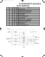
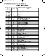
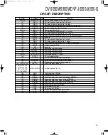
CIRCUIT DESCRIPTION
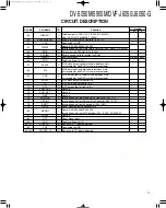
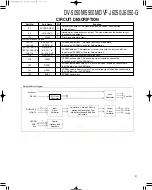
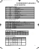
Port No.
Port Name
I/O
Function
1
VDD3
-
Positive supply voltage (+3.3V) for pad ring.
2~8
VIB9~VIB3
I
Connected to digital ground.
9~11
GND
-
Digital ground for core.
12~14
VIB2~VIB0
I
Connected to digital ground.
15,16
DOS1, DOS0
I
Connected to digital ground.
17~19
TEST2~TEST1
I
Connected to digital ground.
20
VDD3
-
Positive supply voltage (+3.3V) for pad ring.
21
VDD2
-
Digital positive supply voltage (+2.5V) for core.
22
AGND
-
Analog ground for D/A converter.
23
DAO Y
O
Y analog output.
24
AVDD2
-
Positive supply voltage (+2.5V) for D/A converter.
25
DAO B
O
Cb analog output.
26
AGND
-
Analog ground for D/A converter.
27
DAO R
O
Cr analog output.
28
AVDD2
-
Positive supply voltage (+2.5V) for D/A converter.
29
VREF
I
Reference voltage input for 3DACs.
30
FSADJ
I/O
Current source for full scale adjustment of 3DACs.
31
AVDD2
-
Positive supply voltage (+2.5V) for D/A converter.
32
VG
O
Compensation pin for gate voltage of DAC current cells.
33
AGND
-
Analog ground for D/A converter.
34
CLMP
O
Unused.
35
SPR7/V09
O
Unused.
36
GND
-
Digital ground for core.
37~39
SPR4/V06~
Multi-purpose parallel output converted from serial data through MPU interface / pixel
SPR6/V08
O
data output.
40,41
VDD3
-
Positive supply voltage (+3.3V) for pad ring.
42
GND
-
Digital ground for core.
43~45
SPR1/V03~
Multi-purpose parallel output converted from serial data through MPU interface / pixel
SPR3/V05
O
data output.
46
SPR0/V02
O
Multi-purpose parallel output converted from serial data through MPU interface (LSB) /
pixel data output.
47
VO1
O
Pixel data output.
48
VO0
O
Pixel data output (LSB).
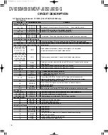
-
Positive supply voltage (+3.3V) for pad ring.
-
Digital ground for core.
I
Address input for monitoring internal register (MSB).
I
Address input for monitoring internal register.
-
Digital ground for core.
I
System clock input (27MHz).
I
System reset input (negative).
-
Positive supply voltage (+3.3V) for pad ring.
-
Digital positive supply voltage (+2.5V) for core.
I
Chip select input of MPU serial interface.
I
Data input of MPU serial interface.
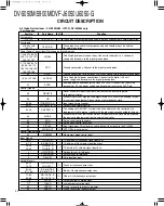
64
SCLK
I
Clock input of MPU serial interface.
65
RMA1
I
Address input for monitoring internal register.
66
RMA0
I
Address input for monitoring internal register (LSB).
67
CKPOL
-
Internal clock. polarity control input.
68
VIA9
I
Pixel port A input (MSB).
69~76
VIA8~VIA1
I
Pixel port A input.
77
VIA0
I
Pixel port A input (LSB).
78
NVS
I/O
Active low vertical sync.
79
NHS
I/O
Active low horizontal sync.
80
VDD3
-
Positive supply voltage (+3.3V) for pad ring.
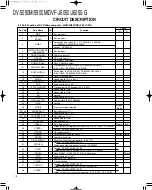
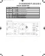
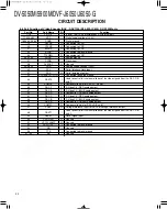
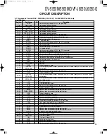
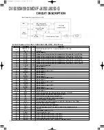
6-7 Progressive Convert DAC : PM0026A (X25, IC601) DV-5050M/DVF-J6050 only
• Port Function
www. xiaoyu163. com
QQ 376315150
9
9
2
8
9
4
2
9
8
TEL 13942296513
9
9
2
8
9
4
2
9
8
0
5
1
5
1
3
6
7
3
Q
Q
TEL 13942296513 QQ 376315150 892498299
TEL 13942296513 QQ 376315150 892498299

