


Section 2: Connections
Model 4200A-SCS Pulse Card (PGU and PMU) User's Manual
2-24
4200A-PMU-900-01 Rev. A December 2020
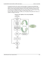
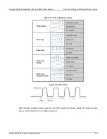
Note that after the first action, "Output Pulse Burst," all pulse channels in the test stop pulsing and
output 0 V while performing the actions in the remaining boxes in the diagram. The time between
pulses is determined by the time required to process the measurements and perform the calculations
and comparisons shown in the previous figure. Wider pulses, longer pulse periods, and a higher
number of pulses increases the time between pulses where the output is at 0 V. Note that both Pulse
I-V and Waveform Capture Test modes use this algorithm and both will output 0 V between pulses for
each step in a sweep. For strict control over the pulse voltage versus time, see the Segment Arb
feature of the PMU.
The "Get Good Measurement" step shown in the previous figure also must ensure that the current
measure range is correct (if ranging is enabled) and check the measured voltage and current against
(on page 3-6).
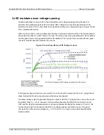
There are two parameters that control how the LLEC algorithm functions: Maximum number of
iterations and tolerance window. For ITMs, the maximum number of iterations is fixed at 20 and the
tolerance window is 0.3 percent. For UTMs, use the
setmode
function. The LLEC algorithm iterates,
trying to reach the target voltage until one of the following occurs:
•
The target voltage is reached (within tolerance specified).
•
The maximum number of iterations is reached. The maximum number of iterations must be equal
for each channel in the test.
Coping with the load-line effect
There are several ways of working with this effect. The simplest one is to program the DUT load into
the pulse card channel using the
pulse_load
function, or setting the Pulse Load value in the
(on page 5-1) virtual front panel. The pulse card will calculate the appropriate V
INT
to output so that
the V
DUT
pulse waveform, specified by
pulse_vlow
and
pulse_vhigh
, has the correct levels. This
works well for high impedance devices or device terminals (R
DUT
= 1 kΩ), such as the gate terminal
on a CMOS field effect transistor (FET). Unfortunately, many times R
DUT
is not known or varies. A key
example of a varying R
DUT
is the drain-source resistance during a V
D
-I
D
sweep, where R
DS
is changing
from point-to-point and sweep-to-sweep.
There is basically only one way to handle this situation, with two different levels of implementation. In
general, assume the DUT is a FET. If the test consists of a single or limited number of gate and drain
test points, the necessary voltages can be determined by pre-characterizing each unique set of test
conditions.
This pre-characterization requires some way to measure the pulse heights, which is typically done
using an oscilloscope and an iterative trial and error approach. Each test voltage needs to be
measured, with the pulse levels adjusted until the correct voltage is reached. Record each pulse level
required to reach the required V
DUT
levels.
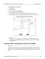
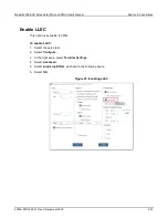
The 4225-PMU has built-in load-line effect compensation. For details, see
compensation (LLEC) for the PMU
(on page 2-21).


