Model 4200A-SCS Pulse Card (PGU and PMU) User's Manual
Section 3: Setting up PMUs and PGUs in Clarius
4200A-PMU-900-01 Rev. A December 2020
3-45
Step 3. Is the pulse level correct for each channel?
1. If the pulse level is not correct for each channel, enable load-line effect compensation (LLEC). To
compensate for the IR drop effect, the LLEC algorithm applies multiple pulses at each sweep step;
make sure that the DUT behavior is not adversely affected by the LLEC approach.
2. Run the test again and compare results. If the results match the test settings, the issue was the
lack of LLEC.
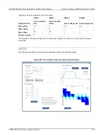
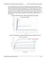
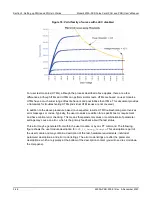
The load-line effect can reduce the voltage level at the DUT terminal when current is flowing. See
Load-line effect compensation (LLEC) for the PMU
(on page 2-21).
Step 4. Is the pulse I-V curve suspect?
(on page 3-45) for examples with LLEC disabled and
enabled.
Step 4. Is the pulse I-V curve suspect?
If the waveform has a good shape (Step 2. Verify the pulse shape), and the pulse level is correct
(Step 3. Is the pulse level correct for each channel?), but the pulse I-V curve is suspect, perform the
steps below.
In this procedure, you set test parameters to provide boundaries for the test envelope. When load-line
effect compensation (LLEC) is disabled, the source voltage must be bounded.
LLEC may not respond properly for a high-gain transistor (for example, a compound
semiconductor-based amplifier or power transistor).
If the pulse I-V curve is suspect:
1. Disable the load line for the gate and drain in the Key Parameters. For an ITM, see
(on page 2-21).
2. Choose the maximum voltage for the selected source range. For example, many high-power
transistors require fairly high voltages and currents, so the PMU 40 V source range is common.
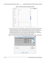
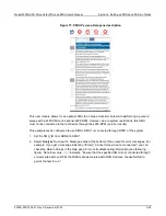
3. Set the thresholds in the All Parameters pane (see following figure and
(on page 3-6) for more detail). Enter the maximum voltage for the DUT. For a
transistor, set the
ThresholdVoltDrain
voltage for the maximum voltage for the drain.

