REL 1.2
Page 59 of 82
i.MX6 Qseven PMIC SOM Hardware User Guide
iWave Systems Technologies Pvt. Ltd.
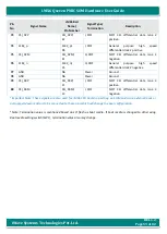
Pin
No
Signal Name
i.MX6 Ball
Name/
Pin Number
Signal Type/
Termination
Description
73
CSI_D2P
CSI_D2P/
E2
I, DIFF
MIPI CSI differential data lane 2
positive.
74
CLK2_p
CLK2_p/
D5
I, DIFF
General
purpose
high
speed
differential clock 2 positive.
75
CSI_D2M
CSI_D2M/
E1
O, DIFF
MIPI CSI differential data lane 2
negative.
76
CLK2_n
CLK2_n/
C5
O, DIFF
General
purpose
high
speed
differential clock 2 negative
77
GND
NA
Power
Ground.
78
GND
NA
Power
Ground.
79
CSI_D3P
CSI_D3P/
F1
I, DIFF
MIPI CSI differential data lane 3
positive.
80
CSI_D3M
CSI_D3M/
F2
I, DIFF
MIPI CSI differential data lane 3
negative.
¹ Important Note: These signals are also used for i.MX6 CPU bootstrap setting on SOM and so no external loads or
pull-up/pull-down resistors to be connected to these pins which will change the boot configuration.
² Note: Termination value is mentioned based on SPI flash as boot media. If boot media is changed to other using
Boot media setting switch (SW1), termination value also may change.


