


S p e z i a l e l e k t r o n i k G m b H
iseg Spezialelektronik GmbH
Email: [email protected]
Tel ++ 49 (0) 351 / 26 996 - 0
Bautzner Landstr. 23
http://www.iseg-hv.de
Fax ++ 49 (0) 351 / 26 996 - 21
D - 01454 Radeberg/ Rossendorf
3
Table of Contents
1
Safety instructions ............................................................................................................................................................ 5
2
Device description ............................................................................................................................................................ 6
2.1
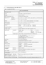
Technical data device class HPS, 300 W ...................................................................................................................... 7
2.2
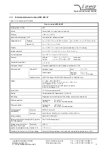
Technical data device class HPS, 800 W ...................................................................................................................... 9
2.3
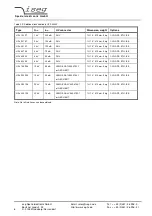
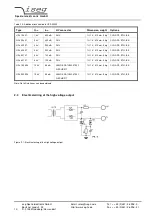
Electrical wiring of the high voltage output ................................................................................................................... 10
2.4
Dimensions .................................................................................................................................................................. 11
3
Functional description ..................................................................................................................................................... 12
3.1
Operation states ........................................................................................................................................................... 12
3.2
Monitoring .................................................................................................................................................................... 13
3.3
Interlock ....................................................................................................................................................................... 14
3.4
ARC Management ....................................................................................................................................................... 14
3.5
KillEnable ..................................................................................................................................................................... 15
4
Pinout ............................................................................................................................................................................. 15
4.1
Supply .......................................................................................................................................................................... 15
4.2
HV connection .............................................................................................................................................................. 15
4.3
OV connection ............................................................................................................................................................. 15
4.4
IL connection ................................................................................................................................................................ 15
4.5
Interface connection ..................................................................................................................................................... 15
5
Operation ........................................................................................................................................................................ 16
5.1
Operating mode ........................................................................................................................................................... 16
5.2
Front panel operation ................................................................................................................................................... 16
5.3
Interface control ........................................................................................................................................................... 19
5.4
Description of the Analogue I/O interface (AIO) ........................................................................................................... 25
6
Troubleshooting .............................................................................................................................................................. 27
6.1
Error messages on Displays ........................................................................................................................................ 27
6.2
Further Errors ............................................................................................................................................................... 27
7
Maintenance ................................................................................................................................................................... 27
List of Figures
Figure 2.1: Electrical wiring of the high voltage output ............................................................................................................ 10
Figure 2.2: Dimensioned drawing, in mm ................................................................................................................................ 11
Figure 3.1: Operating area of the device. ................................................................................................................................ 12
Figure 3.2: Power reduction vs. input voltage ......................................................................................................................... 14
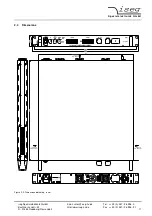
Figure 5.1: Back panel of the device ....................................................................................................................................... 15
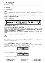
Figure 6.1: Front panel (HV connector at the front) ................................................................................................................. 16
Figure 6.2: Set values the display in HV OFF state ................................................................................................................. 16
Figure 6.3: Set values the display in HV ON state .................................................................................................................. 16
Figure 5.4: Electrical wiring of the analogue and digital in- and outputs .................................................................................. 26


