


Application Note
20 of 63
V 1.2
2018-12-12
5 Output PMIC Controller/ IRPS5401
User guide with DB295 and DB296 demo boards
4.10
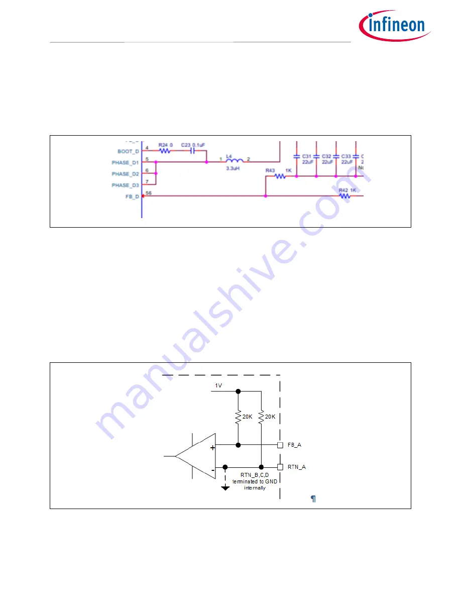
½ Scaling of VOUT
If VOUT is > 2.55 V, VOUT will need to be scaled by 1/2. This means a resistor divider will need to be used to
divide the output voltage by 1/2. This has been done with two 1K resistors on SW-C and D on the demo boards.
VOUT>2.55 V is not just the VOUT_COMMAND value but also VOUT_C OFFSET and MARGIN_HIGH
value.
Figure 26
VOUT scaling
FB_x is not a high impedance input so an error may be introduced due to these resistors. This is an error above
and beyond the error introduced by the tolerance (usually 1%) of the resistors. All FB_x pins are internally
biased up to 1 V with an internal 20 k resistor. So anytime FB_x is not sitting at 1V a bias current will be sourced
or sunk by the FB_x pin. The worst case error will be with VOUT = 5 V. Internally the DAC will be set to 2.5 V and
the FB_x pin will be at 2.5 V during regulation. This will result in IFB_x = (2.5 V-1 V)/20k = 75
µ
A. This additional
current will flow in the upper resistor of the divider (R42 above) and result in and error of 75
µ
A*1 k = +75 mV.
+1.5% error.
At the expense of added power dissipation, the error can by reduced by using lower value resistors. If two 250
Ω resistors are used instead of 1 k, the 75 mV error would be 18.75 mV (0.37% error). But power dissipation
would increase from 12 mW to 50 mW.
Figure 27
FB_x
Alternatively, the upper resistor can be reduced to account for the added bias current. This is best suited for
outputs that would be set and not changed. If R42 was reduced to 976 Ω in the example above and VOUT is set


