


Design guide IDP2303(A)
Tips on PCB layout
Application Note
40
Revision 2.0
2017-05-03
6
Tips on PCB layout
Infineon's digital platform controller IC integrates the PFC and LLC converter controllers in one package.
Therefore, it is a good idea to physically separate the PFC and LLC circuits on the PCB to avoid mutual
interference.
HSGND
HSVCC
HSGD
GD1
CS1
IDP2303
GD0
VCC
GND
HV
VAC
ZCD
VS
CS0
Configuration
HBFB
Vout_1
MFIO
Vout_2
STANDBY
A
B
GD0
GD1
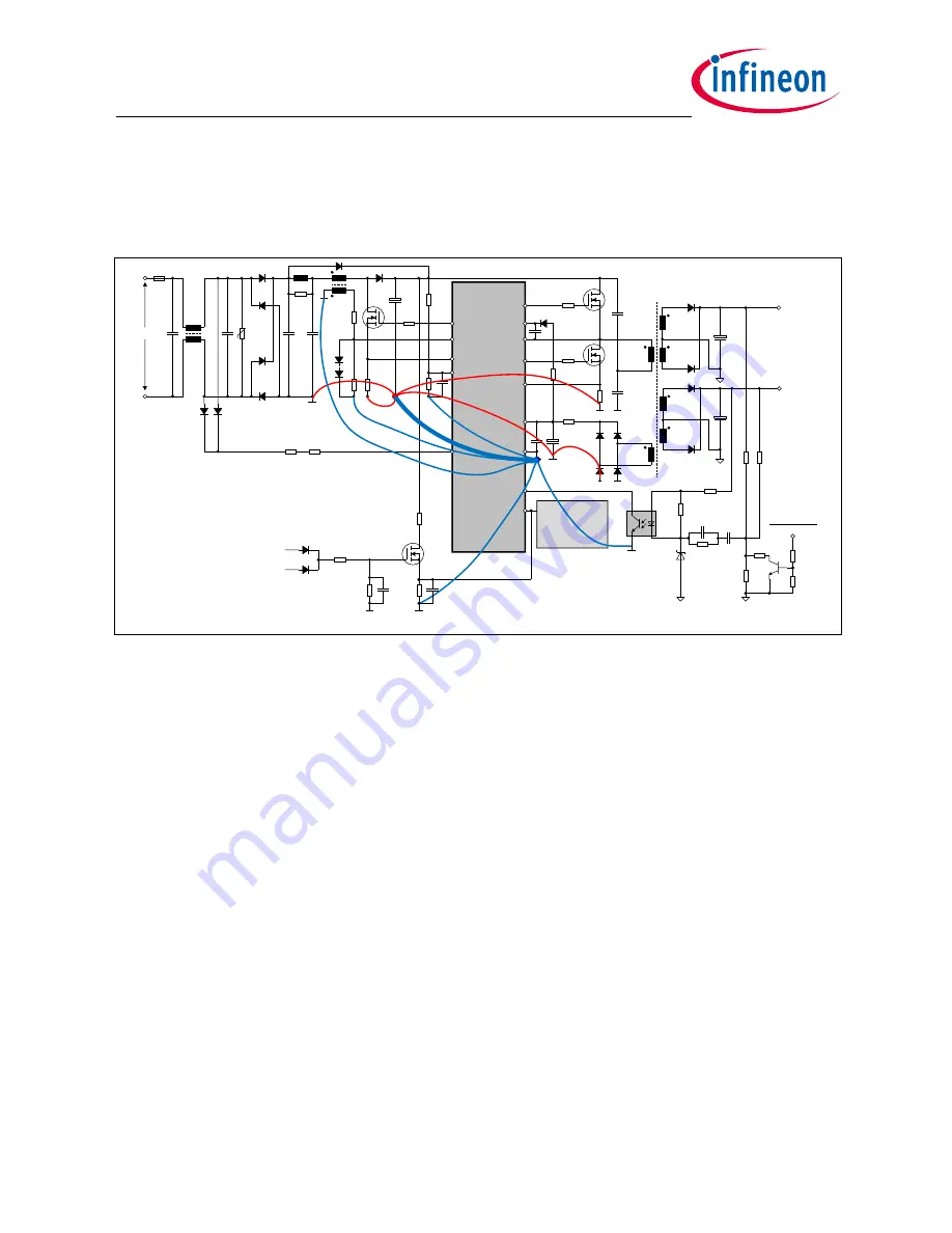
Figure 27
Star connection of grounding
6.1
Star connection of grounding
“Star connection” of grounding (illustrated in Figure 27) is a proven and effective way to minimize the risk of
mutual interference among signals.
The PFC bulk capacitor ground (red point A) is taken as the system ground reference at the primary side.
The other power ground should have direct connections to this system ground reference point, shown as
red lines.
The IC Signal GND, VCC GND, current sense GND, MOSFET/diode heatsink and EMI return GND, shall all be
“star” connected to the PFC bulk capacitor ground directly and the PCB traces should be as short as
possible.
The second ground reference is the ground of the IDP230x IC VCC capacitor (blue point B), which should
be mounted very close to the IC ground. All ground connections of small signals around the controller IC
are connected to the IC VCC ground point, shown as thin blue lines.
The IC ground is connected to the PFC bulk Capacitor ground, shown as a thick blue line.
The PCB ground traces for HBFB, PFCZCD and PFCVS signal are strongly recommended to be separately
connected to the second ground reference, to avoid interference.
In addition, in order to minimize the impedance of the ground PCB trace, it is strongly recommended that
the ground connection PCB traces are as short and thick as possible.
6.2
Filtering capacitors
Filtering capacitors are often used to suppress the high frequency noise. These filtering capacitors, such as
the capacitors for VCC (recommended value 100 nF), PFCVS pin (recommended value 1 nF), LSCS pin


