


Design guide IDP2303(A)
PFC design
Application Note
16
Revision 2.0
2017-05-03
The triggering of OCP protects the PFC inductor from saturation and other components from over current
stress.
The triggering of OCP does not occur during normal operation.
3.3.4.1
Over Current Protection(OCP) tolerance & selection of current sense
resistor
From the datasheet (Table 5), the parameters of the IC that will affect OCP protection tolerance are:
OCP1 threshold tolerance
OCP1 comparator propagation delay
Table 5
Electrical characteristics of the CSx pin
Parameters
Symbol
Values
Unit
Note/Test condition
Min.
Typ.
Max.
OCP, OCP1 threshold tolerance
Δ
V
OCP1
—
—
±6.2
%
Delay from V
CSx
crossing V
CSxOCP1
to CSx_OCP1 rising edge, 1.2 V
range
t
CSOCP1
20
320
620
ns
1
input signal slope
dV
CS
/dt = 10 mV/µs
2
90
170
250
ns
1
input signal slope
dV
CS
/dt = 150 mV/µs
2
90
140
210
ns
1
input signal slope
dV
CS
/dt = 300 mV/µs
2
1
Not tested in production test.
2
This slope represents a use case of a switch-mode power supply with minimum input voltage.
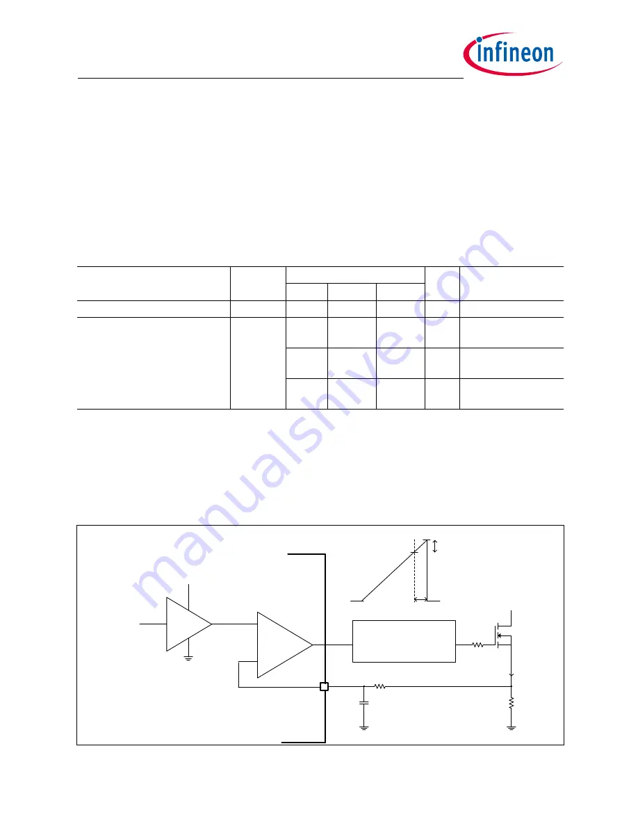
In reality, external circuit specifications also come into play. For example, from Figure 11, it can be seen that
the external parameters affecting OCP protection are:
The gain error caused by the external RC filter
The external delay caused by the RC filter
External propagation delays caused by the gate discharge and MOSFET drain-source capacitor discharge
DAC
OCP
comparator
-
+
PFCCS
R
shunt
i
ocp_power
V
OCP_ref
Digital OCP level
V
OCP_COMP
Propagation delay
(internal IC+ external
RC+external gate drive)
i
ocp_power
i
OCP_level
Δi
t
delay
Figure 11
OCP protection implementation structure


