


Design guide IDP2303(A)
PFC design
Application Note
10
Revision 2.0
2017-05-03
3.2.3.3
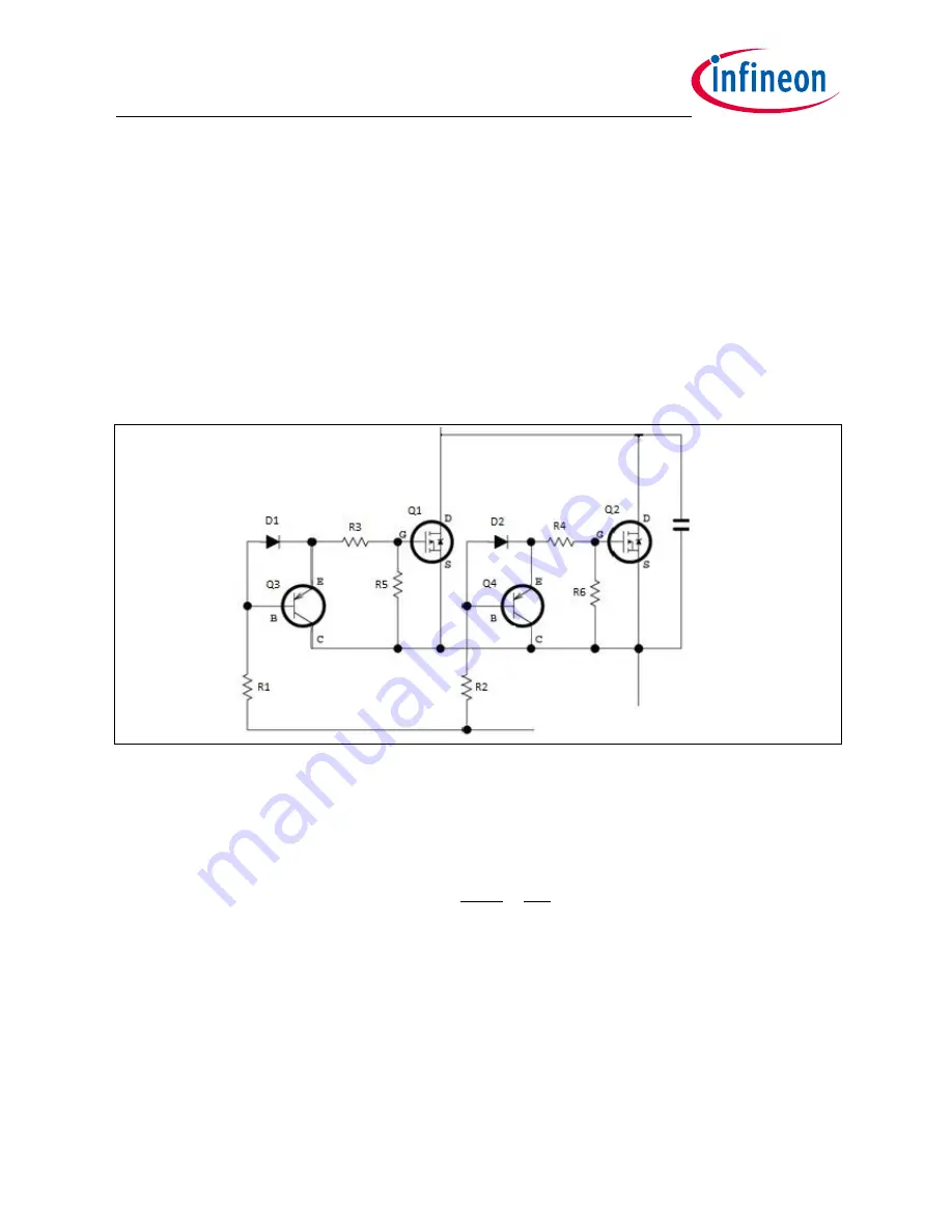
Other design tips for the gate driving circuit
For some high power SMPS applications, two MOSFETs are often connected in parallel for the PFC converter.
In this case, it is recommended to enhance the PFC driving capability by adding an additional circuit close to
the PFC MOSFET, as shown in the example in Figure 6.
During turn-off, transistors Q3 and Q4 are turned on, discharging the PFC MOSFET gate capacitor. As a
result, the turn-off of the MOSFETs is accelerated, which reduces the MOSFETs turn-off losses. Meanwhile,
the turn-on is defined by the constant gate charge current, which can be kept relatively slow for better EMI
performance.
Apart from the gate drive resistance itself, 10 kΩ resistors (R5 and R6) are also commonly connected
between MOSFET gate and source to help damping some overshoot and oscillations and discharge gate
capacitor when there is no gate signal.
Figure 6
PFC gate driving circuit
3.2.4
Boost diode
To select an appropriate boost diode, its thermal characteristic needs to be considered.
The average diode current can be calculated by:
𝐼
𝐷_
𝑎𝑣𝑔
= 𝐼
𝑜_𝑃𝐹𝐶
=
𝑃
𝑜_𝑃𝐹𝐶
𝑉
𝑏𝑢𝑠
=
130
390
= 0.33 𝐴
The total diode conduction loss can be calculated by:
𝑃
𝐷_𝑙𝑜𝑠𝑠
= 𝐼
𝐷_𝑎𝑣𝑔
∗ 𝑉
𝑓
= 0.33 ∗ 0.5 = 0.17 𝑊
3.2.5
Boost inductor
One of the key design considerations for a boost inductor is to ensure the minimum switching frequency is
always higher than 25 kHz to avoid any audible noise. The worst cases are usually at extremes of operation
such as minimum and maximum voltage and during start up and load transients - e.g. twice full power.


