Infineon CoolGaN Manual Download Page 16


Application Note 

16 of 23 

V 1.1  

                                                                                                                                                                                                                                                                     2020-11-09  

CoolGaN™ 600 V half-bridge evaluation platform featuring GaN 
EiceDRIVER™ 


Setup and use 


4.8


Initial checkout 

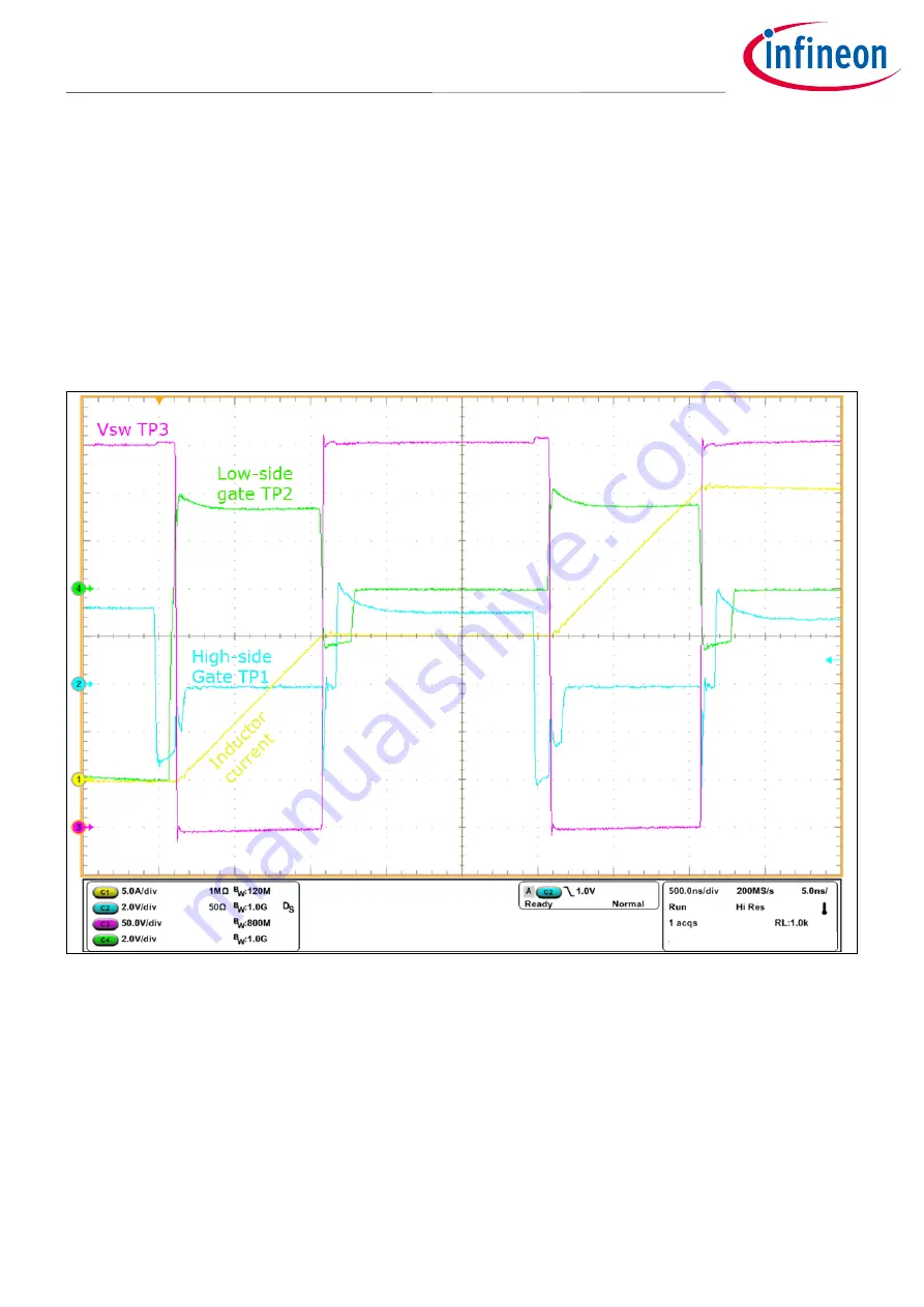
Assuming the board is already setup per section 4.6, the next step is to add an external inductor and bring-up 
the DC bus to operate at the desired test condition. This example shows how to setup the board for double-
pulse testing. In double-pulse testing, first the half-bridge turns on and ramps-up inductor current to a test 
value. Then the primary switch turns-off, and the current freewheels through the other device, which acts as a 
synchronous rectifier. The second pulse shows hard-switched turn-on performance on the leading-edge (at the 
test current) and then continues the ramp to a higher current level. GaN devices perform particularly well on 
these tests because the freewheeling diode has zero reverse-recovery characteristic. Double –pulse testing is 
typically done 1 burst at a time (not continuously) in order to keep power dissipation low, even when testing to 
the voltage and current limits of the device. 


Figure 14


Double-pulse test waveform example 

Connect the external 25 µH inductor and HV power supply as shown in 

Figure 2

Set the pulse generator for a 

pulse-width of 1 µs, and a period of 2.5 µs. setup a 2-pulse burst (refer to 

Figure 14

). It is recommended to set 

the pulse generator for manual mode, where each pulse set is triggered by a button-push. 

Note:


When the low-side switch is operated in the double-pulse test, the default state of the half-bridge 
is that the high-side synchronous rectifier is normally ON. Thus the logic input should be inverted – 
normally high with two pulses going low. Make sure to power-off the HV supply before shutting-off 
the output of the pulse generator: if the pulse generator is powered-off first, it will turn-on the low-
side and ramp the current to uncontrolled value, unless the bus is at zero volts.  

Summary of Contents for CoolGaN

Page 1: ...of EiceDRIVER GaN gate drivers and isolated power supplies for the gate drivers along with input logic that provides adjustable deadtime Using an external inductor the board can be configured for buck...

Page 2: ...mer 6 3 3 Gate drive circuit 7 3 4 Half bridge output circuit 8 4 Setup and use 9 4 1 Test equipment needed 9 4 2 Connections to the terminal block 9 4 2 1 Connections for double pulse testing 10 4 2...

Page 3: ...range up to 450 V limited by the capacitor rating This half bridge can switch continuous currents of 12 A and peak currents of 35 A hard or soft switching Operating frequency can be up to several MHz...

Page 4: ...it Deadtime Circuit Isolated Gate Drive Power Vin Vo Vin PWM 0V Evaluation Board 0 400 V DC Laboratory Power Supply Test Inductor 5 V DC Laboratory Power Supply 50 Pulse Generator Figure 2 Evaluation...

Page 5: ...be set long enough that the high side always fully turns off before the low side turn on with some margin and vice versa A simple adjustable RCD delay circuit generates the deadtime Whenever U11 or U...

Page 6: ...DC DC converter shown in Figure 5 It takes the 5 V input and provides two isolated 8 V outputs VDD1 VSS1 and VDD2 VSS2 A small transformer T1 provides low capacitance isolation and voltage scaling Th...

Page 7: ...e gate RC network described in the datasheet consists of Rx4 Cx4 and Rx5 The small Schottky diode Dx5 provides a low impedance return path for faster gate turnoff effectively bypassing Rx4 Note that t...

Page 8: ...wer supply Attention Normally the bus capacitor is discharged when the lab power supply is switched off But if the power connector is removed while the capacitor is charged not recommended the bus cap...

Page 9: ...a conventional BNC connector you will need a BNC male to MMCX plug cable Fairview Microwave FMC0809315 or a BNC to MMCX adapter Oscilloscope for measurement Due to the fast transient voltage and curre...

Page 10: ...external inductor is connected between Vsw and Vo terminals the circuit is configured as a buck converter If a PWM signal is applied to the PWM input the output voltage will be proportional to the in...

Page 11: ...nductor 5 V DC Laboratory Power Supply 50 Pulse Generator DC Load Figure 9 Connecting the evaluation board in the buck topology Figure 10 shows example waveforms operating in ZVS buck mode at 1 5 MHz...

Page 12: ...V to zero there is a large change in Crss and thus a significant charge injected into the gate approximately 3 nC This charge in a short time I dq dt results in a short current spike that pulls the ga...

Page 13: ...this signal is delayed from TP4 by the deadtime circuit so it has an exponential risetime characteristic Voltage level is standard 5 V AHCT logic level TP1 High side gate voltage signal is the gate of...

Page 14: ...e rising edge of PWM To verify and adjust deadtime connect a 5 V DC supply to the 5 V input on the eval board and connect a pulse generator to the PWM input J1 refer to section 4 3 Set the generator f...

Page 15: ...ly the rising and falling edge deadtimes are set to the same value Turning the trimpots clockwise increases the deadtime Figure 13 Measuring deadtime on the falling edge of PWM 4 7 Test inductor recom...

Page 16: ...zero reverse recovery characteristic Double pulse testing is typically done 1 burst at a time not continuously in order to keep power dissipation low even when testing to the voltage and current limit...

Page 17: ...gh side transistor operating in 3rd quardrant conduction mode You can see the switch node voltage rises several volts above the bus during deadtime due to the effective diode drop across the high side...

Page 18: ...form featuring GaN EiceDRIVER Complete schematic 5 Complete schematic Note Part numbers 1 9 are in the ouput power stage 1x part numbers belong to the high side gate drive 2x are low side gate drive a...

Page 19: ...ng GaN EiceDRIVER PCB layout 6 PCB layout The evaluation board is 1 6 mm thick with 4 evenly spaced copper layers 35 m thick The layer stackup is depicted below Figure 16 Top layer copper layer with t...

Page 20: ...11 09 CoolGaN 600 V half bridge evaluation platform featuring GaN EiceDRIVER PCB layout Figure 18 Lower middle copper layer with top and bottom component overlay Figure 19 Bottom copper layer with bot...

Page 21: ...3 D14 D24 LED GREEN CLEAR 0805 SMD J1 CONN MMCX JACK STR 50 OHM SMD Q1 Q2 Infineon IGOT60R070D1 CoolGaN Transistor R1 R2 RES SMD 499K OHM 1 1W 2512 R11 R21 TRIMMER 1k OHM 0 125W SMD R12 R15 R22 R25 RE...

Page 22: ...aN EiceDRIVER Revision history 8 Revision history Document version Date of release Description of changes V 1 0 2019 01 16 First release V 1 1 2020 11 09 Updates for version B of the driver IC updated...

Page 23: ...intellectual property rights of any third party with respect to any and all information given in this application note The data contained in this document is exclusively intended for technically trai...

Reviews: