57
462
The power supply ground will be connected to Pin 4 (GND) and the DC
output to Pin 3 (+V). See the
Minimum Required Connections
figure in this
appendix for a connection diagram.
S t e p p i n g M o t o r ( Ø A - P i n s 1 & 2 , Ø B - P i n s 5 & 6 )
Motor selection for the OSC-462H/IB462H will have the same recommended
specifications as found in
Section 1.6: Motor Requirements
of this document.
See the
Minimum Required Connections
figure in this appendix for a connec-
tion diagram.
I n p u t C o n n e c t i o n s
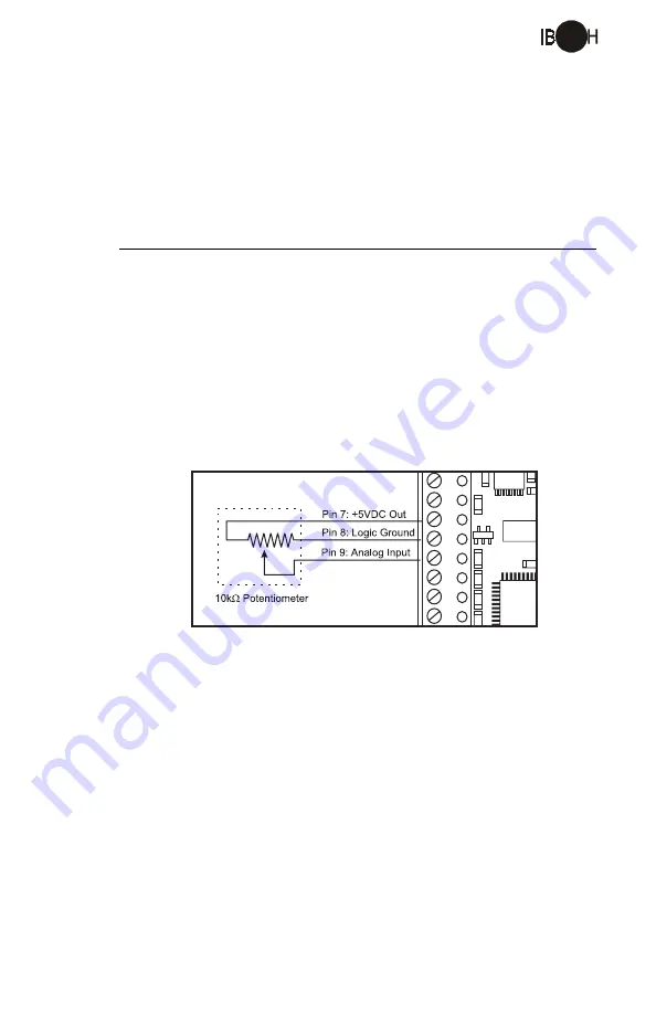
S p e e d C o n t r o l I n p u t ( P i n 9 )
The Speed Control input is the input by which the internal step clock fre-
quency, hence the velocity of the axis, is controlled.
This 0 - 5 volt analog input will typically be interfaced using a 10k
Ω
potenti-
ometer as illustrated in Figure 2.2.7, a joystick wiper or by a 0 to 5V (4 - 20
mA) analog output. If a constant velocity is desired, the speed control input
can be connected directly to the +5VDC output and the desired velocity set
using the VM parameter. When at 0 volts + DB (value of the potentiometer
deadband parameter) the step clock frequency will be at the value specified by
the initial velocity (VI) parameter. When at FS (the value specified by the full
scale parameter), it will be at the value specified by the maximum velocity
(VM) parameter. See
Setting the Initial/Maximum Velocity
, for more details.
R e c o m m e n d e d P o t e n t i o m e t e r
Bourns 53AAA-B28-B15. This is available from Digikey (P/N
53AAA-B28-B15-ND) and Newark Electronics (Stock No.
90F6563).
E n a b l e I n p u t ( P i n 1 0 )
The enable input is internally pulled-up to +5VDC through a 4.99k
Ω
resistor.
When HIGH, or disconnected, the driver outputs are enabled. A LOW will
disable the driver outputs. This input is independent of the step clock input.
This input may be connected by means of a switch between the input (Pin 10)
and logic ground (Pin 8) or a sinking output.
Figure 2.2.7: Interfacing the Speed Control Input with a Potentiometer


