background image

82V3911   WAN PLL

REVISION 1  1/30/15

6

EVALUATION BOARD USER’S GUIDE

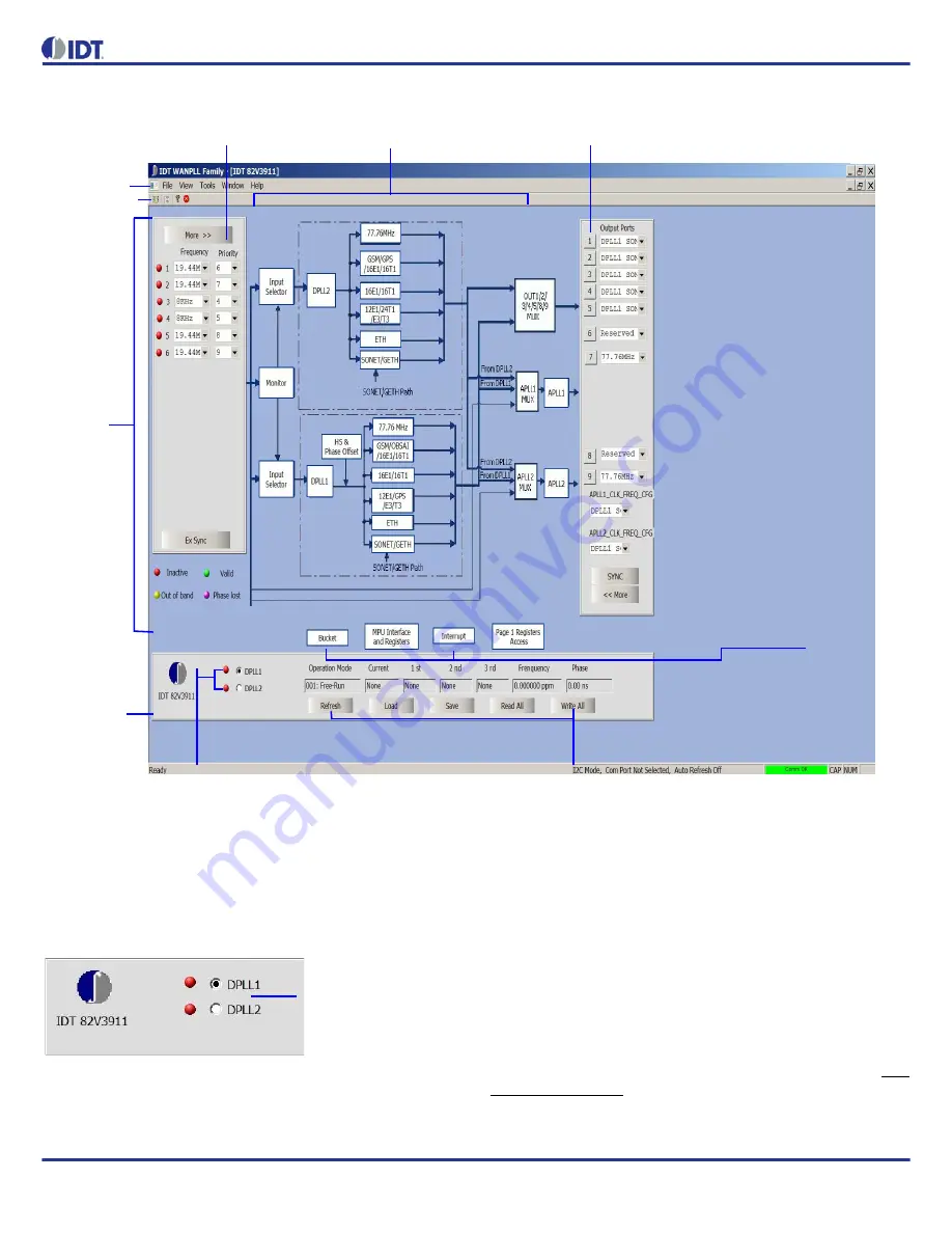
Figure-2   Graphic User Interface (GUI)

2.2.3

DPLL1/ DPLL2 PATH SELECTION

Since some registers are related to the input ports, the DPLL1 and the

DPLL2 are shared paths, and users must select a path (DPLL1 or DPLL2)
before configuring these registers. See 

Figure-3

 for details.

Figure-3   DPLL1/ DPLL2 Path Selection

2.2.4

READ/WRITE THE CONFIGURATION DATA

Generally, once a configuration is made, the configuration data will be

directly written to device. But in the Register Set I dialog box, after config-
uring the registers, you need to click the “Write” or “Write All” button to
write the configuration data to device. 

In the main work area or in the dialog boxes, you can click on the

Refresh” button to read the register value from the device.

2.2.5

LOAD/SAVE THE CONFIGURATION DATA

To load or save the configuration data, please open the Register Set I

dialog box by selecting “Windows > Register Set I” or clicking on “MCU
Interface and Registers”. Or you can click on the Load or Save button in
the Main window. Refer to 

2.9.1 Registers Configuration

 for details.

menu bar

shortcut icons

input ports configuration 

status bar

DPLL1 & DPLL2 path configuration

DPLL1/ DPLL2 path selection

DPLL status indication

output ports configuration

general

configuration

main
work area

click to select DPLL1 or DPLL2 
(currently selected: DPLL1 path)

Summary of Contents for 82V3911

Page 1: ...82V3911 evaluation board user s guide ver 1 0 FEATURES Professional evaluation software to configure and monitor the device Current configuration data can be saved as a file for later use PC REQUIREME...

Page 2: ...Synchronization Control 11 2 5 MONITOR CONFIGURATION 12 2 6 DPLL2 PATH CONFIGURATION 13 2 6 1 DPLL2 Input Selector 13 2 6 2 DPLL2 DPLL 13 2 6 3 DPLL2 DCO Output Clock Frequency Selection 14 2 6 4 DPLL...

Page 3: ...82V3911 WAN PLL REVISION 1 1 30 15 3 EVALUATION BOARD USER S GUIDE 1 HARDWARE CONFIGURATION Figure 1 82V3911 Evaluation Board Illustration...

Page 4: ...tput clock 6 differential 14 Output clock 7 differential 15 Output clock 8 differential 16 Output clock 9 differential 17 Input clock to APLL1 differential 18 Input clock to APLL2 differential 19 Inpu...

Page 5: ...ports configuration area Monitor DPLL2 path configuration area DPLL1 path configuration area Output ports configuration area General configuration area DPLL1 DPLL2 path selection and DPLL status indic...

Page 6: ...to click the Write or Write All button to write the configuration data to device In the main work area or in the dialog boxes you can click on the Refresh button to read the register value from the de...

Page 7: ...r Parameters and Buttons 2 2 7 MENU BAR The menu bar contains five menus as shown in the following File Menu Figure 5 File Menu View Menu Figure 6 View Menu Tools Menu Figure 7 Tools Menu Figure 8 Aut...

Page 8: ...NS The functions of the shortcut icons are described in the following table 2 2 9 STATUS BAR The status bar shows the currently selected microprocessor interface and communication port See Figure 11 f...

Page 9: ...e Open Device or clicking on the shortcut icon Figure 12 Device Port Selection 2 4 INPUT PORTS STATUS AND CONFIGURATION The input ports status and configuration interface is as shown in Figure 13 User...

Page 10: ...d valid register address and bits phase loss indication no activity indication checked no activity hard frequency alarm indication checked has alarm click to pop up the Frame Synchronizing Control dia...

Page 11: ...frame synchronization signal Figure 16 Frame Synchronization Control Dialog Box configuration 0 configuration 1 configuration 2 configuration 3 leaky bucket size upper threshold lower threshold decay...

Page 12: ...limit click to read all registers listed in this dialog box click to pop up the Buckets Configuration dialog box click to exit this dialog box frequency measurement of the hard frequency alarm config...

Page 13: ...t as shown in Figure 19 This dialog box allows users to configure the DPLL2 Figure 19 DPLL2 Dialog Box Note Before opening this dialog box users must select the DPLL2 path see 2 2 3 DPLL1 DPLL2 Path S...

Page 14: ...Selection 2 6 4 DPLL2 SONET GETH CONFIGURATION Click on SONET GETH to select an input source for the DPLL2 SONET GETH See Figure 21 Figure 21 DPLL2 SONET GETH Input Source Selection click to select G...

Page 15: ...e phase detector can not be configured Figure 23 DPLL1 Dialog Box register address and bits DPLL1 Auto Forced input clock selection DPLL1 Internal Fast Slow input clock selection checked Internal Fast...

Page 16: ...ION Click on DPLL1 SONET GETH to select an input source for the DPLL1 APLL See Figure 26 Click on DPLL1 SONET GETH to select a bandwidth for the DPLL1 APLL See Figure 27 Figure 26 DPLL1 SONET GETH Inp...

Page 17: ...ils Figure 27 Output Ports Configuration Shrinked Figure 28 Output Ports Configuration Extended output port number frequency selection Out6 LVDS PECL click to pop up the Out7 LVDS PECL click to extend...

Page 18: ...on APLL1 or APLL2 to configure the APLL interface and setting 19525 to PDSEL and 3124 to M Figure 30 APLL Configuration Interface 3 Click on More in the output ports configuration interface to show al...

Page 19: ...configuration dialog box pops up as shown in Figure 32 Figure 32 Frame Multi Frame Configuration Dialog Box checked 2 kHz 4 kHz 8 kHz register address and bits input clock inverted FRSYNC_8K output co...

Page 20: ...convenient way to access a group of registers that have related functions Figure 34 Register Set II Dialog Box register name register address default value of the register register bits b7 b0 registe...

Page 21: ...Figure 35 Interrupt Dialog Box register address interrupt source status indication red status changed green status not changed interrupt enable disable checked enable register bit interrupt name rese...

Page 22: ...out as shown in Figure 39 Figure 37 Current DPLL Status click to select DPLL1 or DPLL2 Path currently selected DPLL1 path valid input clock with the second highest priority current phase of current DP...

Page 23: ...the scale numbers on the right side of the diagram Show hide the grid lines Setting the data display range of Y axis Setting the data value precision of Y axis Setting the number of grid lines of Y a...

Page 24: ...indow the user can configure the registers in the page 1 See Figure 40 for details Figure 40 Page 1 Register Configuration Click on the button then select the DFS enable Phase Slope Limiting Configura...

Page 25: ...OOHU 1 1 287 287 5HFRYHU ORFN 6RXUFHV N N 336 UDPH 3XOVHV WHUQDO UDPH 6 QF 7 QWHUIDFH 1B 3 7LWOH 6L H RFXPHQW 1XPEHU 5 H Y DWH 6KHHW R I ORFN LDJUDP 6 0 7 9 9 5 9 7XHVGD XJXVW 7LWOH 6L H RFXPHQW 1XPEH...

Page 26: ...WH 6KHHW R I 9 XVWRP HGQHVGD 1RYHPEHU 7LWOH 6L H RFXPHQW 1XPEHU 5 H Y DWH 6KHHW R I 9 XVWRP HGQHVGD 1RYHPEHU 7LWOH 6L H RFXPHQW 1XPEHU 5 H Y DWH 6KHHW R I 9 XVWRP HGQHVGD 1RYHPEHU X X 73 73 X X 21 Q X...

Page 27: ...B 1 1 1 1 9 9 B 1 9 9 B 1 9 9 B 9 9 B 9 9 B 9 9 B 9 9 B 9 9 B 9 9 B 9 9 B 9 9 B 9 9 B 1 9 9 B 1 1 B326 1 B1 B6 1 1 B326 1 B1 1 1 1 287 B326 287 B1 287 287 287 287 287 0 56 1 B B 336 56 1 B B 336 287...

Page 28: ...287 7 B287 7 B 1 7 B287 2 2B3RZHU 9 B2 2 9 9 B 9 B 9 9 9 B 9 9 B 9 9 B 9 9 B 9 9 B 9 9 B 9 9 B 9 9 B 9 9 B 567 26 3 B 2 3 B 2 B6 B6 7 B287 7 B 1 7 B287 7 B 1 7 B287 7 B 1 7 B287 7 B 1 7LWOH 6L H RFXPH...

Page 29: ...9 9 9 B 966 9 966 2 9 2 9 B2 2 9 9 B 9 9 B 9 9 9 9 7LWOH 6L H RFXPHQW 1XPEHU 5H Y DWH 6KHHW R I 3RZHU 1 6 0 7 9 9 5 9 7XHVGD XJXVW 7LWOH 6L H RFXPHQW 1XPEHU 5H Y DWH 6KHHW R I 3RZHU 1 6 0 7 9 9 5 9 7X...

Page 30: ...y of users Anyone using an IDT product in such a manner does so at their own risk absent an express written agreement by IDT While the information presented herein has been checked for both accuracy a...

Reviews: