background image

A N TE NNA  CO N N E CTOR 

Connect  the su ppl ied flex i ble anten na.  An  external anten n a  can be used,  u si n g  a  BNC conn ector. 

T R ANSMI T/BATT E R Y   IN D I CATOR 

I l lu m i nates  in  the transmit  mode.  Also  in dicates  the battery  condit ion;  du ring  transmission.  The 

voltage  of  N i ckel-Cadmium  batteri es  drops  rapidl y  just  before  they  are  exhausted,  so  when  this 

in dicator goes out, be sure to i m m ediatel y stop u sing  it,  and charge the batteries  again. 

CHA N N EL  SELECT  SWITCH 

Selects  on e of the programmed chan nels. 

(1) 

SQUELCH  CO N T R OL 

Sets  the  squ elch  threshold  level.  To  turn  O F F  the squ elch fu n ction ,  rotate this  control  completely 
counterclockwise.  To set  the threshol d l evel  higher,  rotate the  control cl ockwise. 

([.' 

VOLUME  CONT ROL 

and 

POW E R   SW I TCH 

When  the control is turn ed completely countercl ockwise,  the power  is OFF.  By turning the control 
cl ockwise  beyond the  "cl ick'',  the unit  is  tu rned ON  and the audio level increases  by further rotat­

ing  it clockwise. 

"]: 

EXT E R NAL  SPEAKER  JACK 

When  an  external  speaker  (or  an  earphone)  is  used,  con nect  it  to this  jack.  Use  a  speaker with an 

i mpedance  of 

ohms.  When  the  extern al  speaker  is  conn ected  the  bu ilt -in  speaker  does  not 

fun ction. 

!._: 

EXTE R NAL  MI C  JACK 

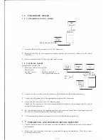
When  an  externa l  microphone  is  u sed,  connect  it  to  this  jack.  See the  schematic for  the  proper 
hookup.  When  the  external  mi crophone  is  connected the  bu ilt-in  m icrophone  does  not  fu nction . 

The  IC-CM9  optional speaker-m icrophone  can  also be used. 

Eloct'ot  oondoMoc  m;ornphon o 

Microphone 

R =20-30Kn 

Dynamic mi crophone 

Microphone 

PTT  SWITCH 

PTT SWITCH 

:8 

.. 

PUSH  TO  TALK  ( PTT)  SW I TCH 

F or  tra nsm ission,  press  this  switch  and  talk  into the  microphon e  with  normal  voice.  The  intern a l  

mi crophone i s  o f  the el ectret-con denser type and provi des  good pickup for all voice l evels . 

CHA R GE R   CO N N E CTOR 

Connects to the output plu g of the wal I  charger CM-25U/E  or other  1 2V DC power  sou rce. 

'\_Q

BATTE R Y   CHA R GE  I N D I CATOR 

Lights during battery charging. 

2-2 

Summary of Contents for IC-H12

Page 1: ...VHF RADIOTELEPHONE 12 channels l C H 2 MAINTENANCE MANUAL...

Page 2: ...6 1 DISASSEMBLY OF THE CASES 6 6 2 DISASSEMBLY OF UNITS 6 2 3 6 3 PTT SPRING ASSEMBLY 6 3 6 4 TOP PANEL CONSTRUCTION 6 4 6 5 UNIT BOTTOM ASSEMBLY 6 5 7 MAINTENANCE AND ADJUSTMENT 7 1 13 7 1 MEASURING...

Page 3: ...o 60 Degrees C 4 Degrees F to 140 Degrees F 50 ohms unbalanced DC 8 4V with attendant power pack IC CM3 DC 6 to 12V negative ground is acceptable Transmitting At 2 5 watts output Approx 700mA Receivin...

Page 4: ...N DICA TO R 1 A N TE N N A CONN ECTOR 6 EXT E R N A L SPEA K E R JACK 8 PUSH TO TALK PTT SWI TCH F R ONT PAN E L SPEAKE R 3 CH A N N EL S ELECT SWITCH 2 1 5 VO L UM E CON TR O L and POWER SWITCH R EAR...

Page 5: ...u rned ON and the audio level increases by further rotat ing it clockwise EXTE R NAL SPEAKER JACK When an external speaker or an earphone is used connect it to this jack Use a speaker with an i mpedan...

Page 6: ...posed of the second local oscillator second mixer limiter amplifier quadrature detector and active filter circuits The second Iocal oscillator oscilIates 10 240MHz with X101 and is fed to the second m...

Page 7: ...X202 for receive with X203 for simplex transmit with X 204 for duplex transmit and the signal at two times this frequency is taken from the collector of 0207 and fed to the mixer of the P L L circuit...

Page 8: ...and oscillates in 70MHz range The oscillator frequency is controlled by a DC voltage which is supplied from the loop filter to varactor diode D203 In the receive mode R 5V is applied to D204 s anode...

Page 9: ...es and twelve channels be progra med into the board 5 is applied o a channel line one of channel 1 channel 12 through the channel select switch and ed to BCD codes by diodes programmed into the board...

Page 10: ...tch Low Pass 0209 0211 0212 0213 f f D216 D217 2SC2668 2SC383 2SC2053 2SC1947 Filter 1SS53 x 2 Battery Mute Switch Pack X202 R tj X2 0210 2SC2458 l Crystal Crystal OSC PLL Mixer Low pass 0214 X203 Sim...

Page 11: ...C9122 Programmable Divider IC102 BA526 AF Power Amp IC101 MC3357 IF Circuit IC L107 Quadrature Coil Fl102 455KHz Ceramic Filter X101 10 240MHz 2nd LO Crystal C291 PA Output Trimmer C290 PA Output Trim...

Page 12: ...ck 2 Remove two screws A on the rear panel and four screws on the bottom as shown in the figure 3 e o e t e front panel as shown i n the figure At this ti me be o damage the engaged parts at the top c...

Page 13: ...els remove the rear panel then u plug the connectors between the ma trix board and P L L board and tilt the matrix board as shown e fig ure ish o remove the matrix board from the set unplug the two co...

Page 14: ...S I DE CONTACT H O LDE R CO TACT SPR I N G 41 737 41 750 6 3 PTT SPR ING ASSEMBLY HOW TO REPLACE PTT SPRING e PTI spring is soldered at its top as shown in the figure 2 e o e the old spring by heatin...

Page 15: ...061 r f h TOP PANEL 30282 CHASSIS A B 30284 l WASHER R1 VOL J K12181003E5N 1111 10KA L R2 SOL K1214014 5N1212 10KB OR K121B1003E5N1111 10KB 2 5 1 NUT 13 5 1 NUT 1 b TOP PANEL CHASSIS A B c i WASHER J2...

Page 16: ...screws as shown 2 Remove the contact spring by removing the two screws as shown 3 Set the new contact spring so that the split of the spring is on the positive side and the other end on the negative s...

Page 17: ...ITY FREQUENCY RANGE OUTPUT VOLTAGE 50KnNolt or better MEASURING RANGE FREQUENCY RANGE MEASURING RANGE MEASURING RANGE FREQUENCY RANGE IMPEDANCE SWR OUTPUT FREQUENCY OUTPUT VOLTAGE DISTORTION FREQUENCY...

Page 18: ...ly counterclockwise 3 Connect the RF output of a VHF signal generator to the ANT connector 4 Adjust the VO L control and the AF voltmeter range S G BNC 0 Adjust the VO L control for a full scale readi...

Page 19: ...lector base and emitter of each transistor 9 When checking a transmission problem it is convenient to short circuit an accessory mic connector plug and insert it turning on the transmitter 7 4 HOW TO...

Page 20: ...7 5KHz 5Vp p squarewave is not observedat B measure DC voltage on Pin 5 of IC203 if no oscillation 3 Wave measure the output of C and D with an oscilloscope 4 Measure DC voltage of 0201 0202 0203 020...

Page 21: ...jus L216 for maximum voltage P P value on the oscilloscope and then ss on adjus L215 to maximum Set the channel select switch at a high edge fre e a d repeat adjustment of L215 L216 several times Afte...

Page 22: ...O Applying over 10 SV can damage the P A transistor Se e channel select switch at a programmed channel hrough L222 and C285 C286 C290 and C291 for maximum power output while s i g P T s i ch rren drai...

Page 23: ...ect switch at a programmed channel center frequency of the operating fre e cy ange is recommended Adjust L217 and L218 for maximum output on an RF voltmeter 2 2c ed o R257 re se e channel select switc...

Page 24: ...SP terminal Connect a 50 ohm dummy load to e a ten a erminal All receiver spurious should be supressed less tha 3dB over entire frequency a c ecei e udio Output a illivoltmeter oscilloscope an a dist...

Page 25: ...be s represent diode position P P n BCD x 100 BC D x 10 BC D x 1 0 o e 0 requenc 147 995MHz 148 000MHz 148 005MHz 148 010MHz See on The Table of Frequencies and numbers to be utilized on the IC H12 E...

Page 26: ...4 210 485 366 212 515 368 21 545 370 23 216 575 372 265 218 605 374 295 220 635 376 325 222 665 378 22 i 695 380 38 226 725 382 228 755 384 230 785 386 232 815 388 23 845 390 3 236 875 392 238 905 394...

Page 27: ...12 890 392 220 214 920 394 250 216 950 396 280 218 980 398 310 220 154 010 4 00 3 0 222 040 402 370 224 070 4 04 400 226 100 406 30 228 130 408 6 0 230 160 410 490 232 190 412 520 234 220 414 550 236...

Page 28: ...456 875 458 905 460 935 462 965 464 995 466 155 025 468 055 470 085 472 15 474 5 476 75 478 205 480 235 482 265 484 295 486 325 488 355 490 385 492 5 494 5 496 5 498 5 500 535 502 565 504 _59 506 6r 5...

Page 29: ...r SQ L C LO SED SQL OPENED 0 6 0 0 7 8 GND Squelch Control 0 0 7 8 t 7 4 0 7 2 I Squelch Control 4 7 4 7 2 1 S 4 r T R S itch 1 7 0 5 I 8 4 1 7 Regulator __ __ _ _ 4 1 _7 S r 9 I 4___Regul t r__ G D 0...

Page 30: ...4 0 1 4 4 0 1 4 4 0 0 i 0 I 0 GND f 1 56 SMHz J P L L _ _ _ _ _ I C _ 20 _ 2 0 4 0 1 o 4 9 4 9 0 2 4GN D r f l p 1c203 o 9 1 4 1 a o 4 9 o r2A j24 GND I I 1 I I _ ___l_____l_ 1__ IN R E CE IVE MO DE...

Page 31: ...s Reverse polarity of batteries IC CM4 O K Opened wire b etween terminal and power switch or defective pO Ver S Vitch Check QI 1 7 QI 1 9 Q I 2 0 0 1 04 etc of M A I N u n i t N O 1 0 1 Bad contact of...

Page 32: ...E S Y E S Che voltage of IC 01 P L L unit 10 b u t cannot resolve it Y E S Refer to N O POWER O N Y E S Defective X 2 0 I P L L unit Defective X 202 PLL unit Defective IC20 I P L L unit 1 0 2 N O Defe...

Page 33: ...old soldering between Ai T con n ec tor and M A I u nit u t cannot resolve it Replace the wires or resolder them Loe k is failed Refer to LOCK FAILU R E Defective Q 2 0 8 PLL unit YES Defective XI 0 I...

Page 34: ...r NO i Replace the wires or resolder them N _ o _ _ _ _ Lock is failed Refer to LOCK FAILU RE NO NO NO N O Defective Q 2 0 8 P L L unit Defective Q209 PLL unit Defective Q 2 1 2 PLL unit Defective Q 2...

Page 35: ...Supply Voltage VIN Input Voltage TOPR Operating Temperature TSTR Storage Temperature PIN CONNECTION BLOCK DIAGRAM 100 SOOKn 0 1 z 5 N M N Cl 0 0 U U U U ID RATINGS 1 0 0 3 Yoo 0 3 30 7 5 5 5 1 2 5 BCD...

Page 36: ...Supply Voltage VIN Input Voltage TO P R Operating Temperature TSTG Storage Temperature BLOCK DIAGRAM Vee 455 K H Z F I LT E R PL CO rNECTION LIMITER INPUT DECOUPLING S 1 1 2 RATINGS 1 2 4 to 8 1 0 30...

Page 37: ...S Ta 25 C I SYM BO L DESC RIPTION I DD Supply Voltage I Input Voltage TOPR I Operating Temperature TsT R Storage Temperature PIN CONNECTION BA 5 26 I LJ LJ O D D D D D D N 0 C 0 x x 0 0 z 0 0 0 0 0 x...

Page 38: ...or 100K S1 J E L R 10 I 1A R 103 Resistor 100S1 J E L R10 28 R 105 Resistor 56S1 J E L R 10 1C R106 Resistor 220S1 J E L R 10 l C I C101 IC MC3357 2D R107 Resistor 47KS1 J E L R 10 2C IC102 I C BA526...

Page 39: ...R 1 0 4E C 1 34 Ceramic 47 0pF 50V 1 E 7Kr2 J E L R 1 0 4E C 1 35 Electrolytic 1 F 50V RC2 3C 3 3 n J E L R l 0 4E C1 36 Electrolytic 0 47 F 50V RC2 40 2 2KS1 J E L R 1 0 4F C 1 37 Electrolyitc 1 F 50...

Page 40: ...A 136 4A L229 Inductor LA 135 4A L230 Inductor LA 143 4A L231 I nductor L R 77 3E L232 Inductor L R 118 30 R202 I Resistor 39K 2 J E L R10 2F R203 Resistor 12K 2 J E L R 10 2E R204 I Resistor 10K 2 J...

Page 41: ...ramic 0 5p F 50V I 4 E C279 Ceramic 8p F 50V 4 E 0 0 F 50V 3F C280 Ceramic 470p F 50V 4F SS 5X 1EM C281 Ceramic 470p F 50V 4E ic 22 F 1OV MS9 2F C282 Ceramic 47p F 50V 4E Cera 470p F 50V 3E Cera c 470...

Page 42: ...Resis or 1KS J R10 1E R402 Resis or 2 2KS J R10 1E R403 Resistor 10KS J R10 10 R404 Resistor 100 n J R10 3E R405 2 2KS J R10 3B R406 2 2KS J R10 10 2 2KS J R10 3B 2 2 J R10 3B 2 2 J R10 3 C 2 2 J R10...

Page 43: ...I C121 J ol PTT S I R O Tl 8 Rl 5 J R117 J Q 116 Q115 1 2J 3 4 5j1 6 Receiv 3 3 5 f 3 9 3 3 3 3 3 f S 11elclled 0 0 0 0 0 0 Transmit 0 0 0 0 0 0 R 67 912 1 Q 128 RO __ 111 Tl 1 t 1 e Cf63 _ _ _ _ _ v...

Page 44: ...R 51 6 122 p L 05 R 47 6 1 co R O T4 0 Ai Q 103 R 05 9 1 1 8 4 R6 0 T O e 121 8 10 1 9 3 C 08 Q 102 Q tOI RS 6 T O 9 101 9104 06 4 9 sv R4 2 14 6 LoeIced RO S R 24 T 0 1 fJ 120 Q l 8 Q l 7 a 4 R O I...

Page 45: ...DUP T SV J SIMP 8107 12oa 0 8 160 llS _ J S If LJI4 8V V P P fOJ 2 2 e10 xr l IC203 J Cl X201 X2DI 6 4 MHZ fl 820 1 R23f 1 DNS fin4 BV D204 20 R4 8 TO lf O T Si I 4 3 R O T Dup 4 1 T 3 RO R24S R8 4 R2...

Page 46: ...o R21 3 Jn 1 _ L Ttoomv v _ L211 X202 D210 lf214 0 6 C231 204 r _ 0 __ fi 20 6 I L I4oomr II II II Q 212 RO ra6 R J T0 4 XZ02 38 8Z75 HHz X203 7 5 0 12S HHz X204 36 351 MHz Q213 234 R O T4 8 9 4 5V Gl...

Page 47: ...o n o Cl3B J 3 CU1 5 0 001 Rl37 ZZK RIZ O K RIZB 4 7k R 34 lSK Ct33 4 7 R l l I I K p N N C 26 O zz f _ a RllB S 6 K i T Rl 6 J30 K Rf a ZZK Ct32 0 001 CIZ3 0 1 p t l N N C ZI IZOP 47K V V v _ c11s a...

Page 48: ...R o _ K c 2 _ 0 _ 5 Y l I 84 B Q v 1r g g 9 ti a N40 r t t f l l __ __ j j __ 1 l w __ l 1 l 1 9 83 IC ZOI U v V P l V MOD R409 2 21 czo6L I B Bz N ZO R4 08 z ZK1 CZo Yt 7 6 N O N B R40 7 Z ZK czoaYJ...

Page 49: ...MATRIX UNIT CH 11 CH 10 CH 9 CH CH 7 CH 6 I CH 5 CH 4 CH 3 CH 2 CH 1 A B N c c 02 c E 0401 0 i z z 8 3 N z Q CK 12 CH11 CH10 H9 CH 7 CH6 CH 4 CH 3 CH 1 D E...

Page 50: ...PLL UNIT IL w c 8 2 0 0...

Reviews: