background image

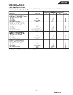
AN8814SB

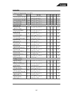
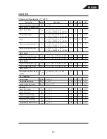
Electrical Characteristics at T

a


=


25

°

C (continued)

Parameter

Symbol

Conditions

Min

Typ

Max

Unit

Thermal protection circuit

Operating temperature

T

THD

180

°

C

equilibrium value

Operating temperature

T

THD

45

°

C

hysteresis width

Design reference data

Note) The characteristics listed below are theoretical values based on the IC design and are not guaranteed.

Usage Notes

1. Avoid the short-circuits between output and V

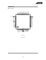
CC

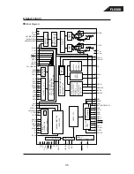
 , and between output pin and GND.

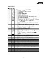
Otherwise, the IC is likely to break down or emit smoke.

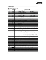
2. An appropriate prior study should be done for use of dip soldering.

Application Notes

P

D


 T

a

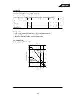
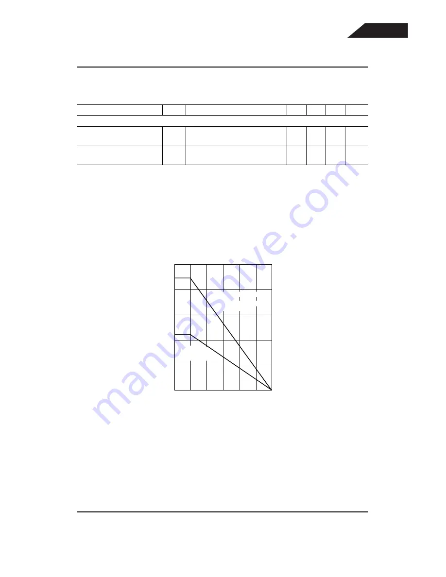
 curves of HSOP042-P-0400

P

D


 T

a

0.000

0

25

50

75

100

125

150

2.500

1.500

1.000

2.240

2.000

1.042

0.500

Ambient temperature   T

a

 (

°

C)

Po

wer dissipation

   P

D

 (W)

Mounted on standard board
(glass epoxy: 
 75 mm 

×

 75 mm 

×

 t1.6 mm)

R

th(j-a)


=

 55.8

°

C/W

Independent IC
without a heat sink
R

th(j-a)


=

 119.9

°

C/W

FL8380

48

Summary of Contents for FL 8380

Page 1: ...STALLATION CONNECTIONS 10 OPERATION 11 BASIC TROUBLESHOOTING 13 TEST PROCEDURE 14 CIRCUIT DESCRIPTION 17 BLOCK DIAGRAM 21 GENERAL UNIT EXPLODED VIEW I II 22 TECH TIP HKTT2003 06 26 DETAILED TROUBLESHOOTING 27 SEMICONDUCTOR IDENTIFICATION 33 PRINTED ClRCUlT BOARDS 59 ELECTRICAL PARTS LIST 61 MECHANICAL PARTS LIST 63 SCHEMATIC DIAGRAMS 68 PACKAGE 72 harman kardon Inc 250 Crossways Park Dr Woodbury N...

Page 2: ...m coming from the pickup or allow it to strike against your skin This compact disc player uses a pickup that emits a laser beam The laser beam is emitted from the location shown in the figure When checking the laser diode be sure to keep your eyes at least 1 foot away from the pickup lens when the diode is turned on Do not look directly at the laser beam CAUTION Using controls and adjustment or do...

Page 3: ... can be damaged by electrostatic discharge from your clothes or your body Proper electrostatic grounding for service personal is required during servicing BEFORE REPAIRING THE COMPACT DISC PLAYER Preparation Human Body Grounding Many of the components used in this compact disc player including the laser pickup are sensitive to electrostatic discharge Service personal should be grounded with an ele...

Page 4: ...16 7 lbs 7 6kg Depth measurement includes knobs and buttons Height measurement includes feet and chassis All features and specifications are subject to change without notice Harman Kardon is a registered trademark and Power for the digital revolution is a trademark of Harman Kardon Inc HDCD High Definition Compatible Digital and Pacific Microsonics are either registered trademarks or trade marks o...

Page 5: ...UDIO SPECIFICATION Typical Limit Output Level 1KHz 0dB no HDCD 1 0 Vrms 1dB Output Level 1KHz 0dB HDCD output 2 0Vrms 2dB Frequency Response 20Hz 20KHz reference 0 1dB 0 5 1 5dB THD 1KHz 0dB 30KHz Filter 0 01 0 05 THD 1KHz 0dB no any filter 0 03 0 08 THD 20Hz 20KHz 0dB 30KHz Filter 0 04 0 05 S N 1KHz 0dB A weighted A Filter 97dB 93dB Dynamic Range 95dB 90dB Channel Separation 1KHz 0dB 30KHz Filter...

Page 6: ...ss one side of this but ton to search forward or the other side of the button to search backwards through a disc to locate a particular portion of the disc being played 8 Skip Button Press one side of this button to move to the next track Í or the other side of the button to move back to the previous track Ífifi on the disc being played 9 Stop Button Press this button to stop the disc currently be...

Page 7: ...ct this plug to an AC outlet If the outlet is switch controlled make certain that the switch is in the ON position Coaxial Digital Output Connect this jack to the coaxial digital input of a digital audio video receiver or an external digital to analog converter for direct access to the digital signals of the FL 8380 DO NOT connect this jack to the standard audio inputs of any device Remote Control...

Page 8: ... n n n o n n n n n n DISC SKIP POWER OFF ON p a Disc Select Buttons b Numeric Buttons c Clear Button d Search Buttons e Skip Buttons f Stop Button g Play Button h Random Button i Pause Button j Program Button k Time Button l Intro Button m Repeat Button n Disc Skip Buttons o Power On Button p Power Off Button Remote Control Functions FL8380 ...

Page 9: ...sc will resume play from the point at which it was paused j Program Button This button is used to program the playback of a disc in a particular order See page 13 for complete instructions on programming the FL 8380 k Time Button In normal operation the display will show the running time of the track being played Press the button once to check the time remaining for the track in play Press the but...

Page 10: ...mote and sliding it back towards the top of the remote NOTE When replacing batteries it is always a good idea to replace both at the same time When the unit will not be used for an extended period of time it is also a good idea to remove the batteries so that the potential for corrosion or damage is avoided If the FL 8380 is installed behind a cabinet or other obstruction that may block the path b...

Page 11: ... to the right of the disc number The icons for all other tray positions that have a disc will be a blue line If the center disc posi tion is empty when the drawer is closed the unit will search for the next position with a loaded disc and place it in the Ready mode The drawer may also be closed and the FL 8380 put into play by pressing the Play Pause button g This will put the disc in the cen ter ...

Page 12: ...tracks will play from that disc This pattern of a randomly selected disc and the play of two random tracks from each disc will continue until all tracks on all discs have been played At that point the unit will stop HDCD HDCD which stands for High Definition Compatible Digital is a sophisticated process that enables the FL 8380 to deliver outstanding digital to analog decoding no matter what type ...

Page 13: ...bel side faces up Moisture inside unit Leave the unit turned ON for 30 minutes to allow moisture to evaporate Play indicator lights but no sound is heard Receiver or preamp and amp Turn on all necessary equipment not turned on Poor connections Make certain connections are secure and made to Wrong source selected the correct e g CD input Select CD source on receiver or preamp Sound skips or stutter...

Page 14: ...r to LEVEL mode 3 Select track 2 of the test disc and play the CD disc 4 The output voltage and gain of the R L channels are taken by pressing the respective buttons on the control board of Audio Analyzer Frequency Response 1 Set the mode of the filter to reference level mode 2 Select the track 3 4 5 and 6 of the test disc and run it under Play mode 3 Check the output of the R L Channels Total Har...

Page 15: ...dio analyzer to DIST Mode 3 Set the unit of the audio analyzer to dB mode 4 Play track 17of the test disc 5 The dynamic range should be A 60dB Channel Separation 1 Set the mode of the filter to DIST CH SP mode 2 Set the audio analyzer to LEVEL mode 3 Play the tracks 8 9 10 11 4 The measured results is the difference between L R channel De emphasis 1 Press the THRU button of the CD filter 2 Play th...

Page 16: ...al Limit Black Dot TCD 725B 1000um 600um Interruption MCD 131 900um 600um Finger print 75um 65um Vertical Deviation MCD 151 0 92mm 0 92mm Eccentricity TCD 712 140um 140um 8cm test disc TCD 783 Last Track Last Track Access Time 1st to last track YEDS18 4 sec 10 sec FL8380 16 ...

Page 17: ...balance voltage VTBAL from Pin 31 VTBAL varies with reference to the center voltage VREF2 1 65 V within 0 5 V The tracking gain will change according to the type of disc For normal disc or CDR disc VGCTRL is set to VREF2 for CDRW disc VGCTRL is set to VREF2 0 75 V At the same time the focus gain is changed too A B C D F PDIC E 32 31 28 21 30 23 25 24 GCTRL To Focus System TBAL Subtraction R10 TEN ...

Page 18: ... voltage VFBAL from Pin 30 VFBAL varies with reference to the center voltage VREF2 1 65 V within 0 5 V The focus gain will change according to the type of disc For normal disc or CDR disc VGCTRL is set to VREF2 for CDRW disc VGCTRL is set to VREF2 0 75 V At the same time the tracking gain is changed too A B C D F PDIC E 36 34 28 29 27 26 GCTRL FBAL Subtraction R7 FEN C4 FEOUT VGCTRL C2 C3 R6 VFBAL...

Page 19: ...l types of disc C38 connected to Pin 9 is for the AGC loop filter The RF Detection block detects the amplitude of the RF signal inputted from the EQ block Inputted RF signal is detected after passing through a high pass filter Detection level is changed in accrodance with the voltage of GCTRL Pin 28 The ENV detection block detects the fluctuation of the 3T composition in the RF signal which is nee...

Page 20: ...ntrolled current for getting regular output power thus the APC Auto Power Control circuit is composed Reference Power Supply A reference power supply for servo is built in The current capacity of the reference supply is about 3 mA VREF1 1 2 VCC1 2 5 V VREF2 1 2 VCC2 1 65 V where VCC1 5 V and VCC2 3 3 V 19 LD 2 1 VCC1 PD 170mV LASER UNIT C33 R18 Q1 LDON 20 R VCC1 R R 2 VREF1 22 R VCC2 R R 2 VREF2 2...

Page 21: ...FL8380 ...

Page 22: ...FL8380 ...

Page 23: ...FL8380 ...

Page 24: ...FL8380 ...

Page 25: ...FL8380 ...

Page 26: ...alignment of the top cover and the rear panel When the screws are tightened on the top cover at the rear of the unit the CD mechanism may warp upward in the area of the clamper arm which causes a Will not Play symptom which shows up as an unusual delay with the word Disc in the display after the Play button is pressed Solutions Washers can be added to the top rear screws to fill the gap between th...

Page 27: ...FL8380 27 ...

Page 28: ...FL8380 28 ...

Page 29: ...FL8380 29 ...

Page 30: ...FL8380 30 ...

Page 31: ...FL8380 31 ...

Page 32: ...FL8380 32 ...

Page 33: ...ta CRC check Built in subcode Q data register CIRC error detection and correction C1 decoder duplex error correction C2 decoder triplex error correction Built in 16 K bits of RAM for use in de interleaving Audio data interpolation Averaging or retention of previous values Digital attenuation 12 dB Audio data peak level detection function Digital audio interface EIAJ format Audio data serial interf...

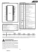
Page 34: ... WVEL PLAY PLLF2 BCLK LRCK SRDATA DV DD1 DV SS1 TX MCLK MDATA MLD SENSE FLOCK TLOCK BLKCK SQCK SUBQ DMUTE STAT RST SMCK PMCK LDON BDO RFDET TRCRS OFT VDET RFENV TE FE TBAL FBAL VREF FOD TRD KICK ECS ECM PC TVD TRV 61 62 63 64 65 66 67 68 69 70 71 72 73 74 75 76 77 78 79 80 40 39 38 37 36 35 34 33 32 31 30 29 28 27 26 25 24 23 22 21 60 59 58 57 56 55 54 53 52 51 50 49 48 47 46 45 44 43 42 41 1 2 3 ...

Page 35: ...LDON PLAY FLOCK TLOCK 40 42 11 12 26 KICK 21 TRV 16 DMUTE 1 BCLK 3 SRDATA 2 LRCK 23 PC 24 ECM 6 TX 64 IPFLAG 65 FLAG 22 TVD 27 TRD 28 FOD 31 TBAL 30 FBAL 43 WVEL 10 SENSE STAT X1 X2 MSEL CSEL PMCK FCLK SMCK VCOF2 58 79 77 59 20 63 19 CK384 EFM 54 VCOF 49 MDATA 8 MCLK 7 MLD 9 17 44 46 45 47 41 52 76 78 RSEL ARF PSEL DSLF PLLF2 48 PLLF 62 13 67 66 55 56 68 15 14 80 CLDCK BLKCK SUBC SBCK FLAG6 RESY 6...

Page 36: ...de block clock signal fBLKCK 75 Hz 14 SQCK I External clock input for subcode Q register 15 SUBQ O Subcode Q data output 16 DMUTE I Muting input Effective only for an output bit rate of 64 fs H level muting 17 STAT O Status signal CRC CLVS TTSTOP JCLVS SQOK FLAG6 SENSE FLOCK TLOCK rpm data and FCLV 18 RST I Reset input L level reset 19 SMCK O If MSEL is H level 8 4672 MHz clock signal output If MS...

Page 37: ...tput fPCK 4 3218 MHz or DSLB 54 VCOF2 I O VCO loop filter pin 55 SUBC O Subcode serial output 56 SBCK I Serial clock input for subcode serial output 57 VSS I Ground for oscillator circuit 58 X1 I Crystal oscillator circuit input output pins f 16 9344 MHz 33 8688 MHz 59 X2 O Crystal oscillator circuit output output pins f 16 9344 MHz 33 8688 MHz 60 VDD I Oscillator circuit power supply 61 BYTCK or ...

Page 38: ...channel audio outputs 73 OUTL O Left channel audio output 74 AVSS1 I Ground for analog circuits common use for left and right channel audio outputs 75 OUTR O Right channel audio output 76 RSEL I RF signal polarity selection pin H level bright level is H L level bright level is L 77 VCC5V I 5 V power supply applied to pins for 5 V input 78 PSEL I When IOSEL is H level test pin Keep this at L level ...

Page 39: ... band RF amp and AGC which meet CAV playback with 24 times speed or more Features Variable equalizer which meets CAV playback with 24 times speed or more CAV playback Wide band RF amp and AGC fC 20 MHz or more 3 dB Balance adjustment function built in Focus error amp tracking error amp CD RW playback compatible Variable gain Focus error amp tracking error amp to 16 9 dB OFTR BDO detection APC amp ...

Page 40: ...TRL 28 FBAL 29 TEN 24 TEOUT 25 CROSS 21 CCRS 23 TBAL 30 VCC2 7 VCC1 4 GND 18 V REF1 20 BDO RF AGC BCA RFDET AC EQ ADD amp Amp 32 35 36 V REF2 22 PD 1 LD 2 FEOUT 27 FEN 26 OFTR 16 COFTR 15 BDO 14 CBDO 13 OFTR Amp Comp BCA GCA ADD amp Amp GCA 33 34 ADD amp 31 Amp BCA BCA GCA GCA ENV detection FL8380 40 ...

Page 41: ... HPF of AGC input 9 AGC loop filter connection pin 10 AGC output pin 11 Capacitor connection pin for HPF amp 12 3TENV output pin 13 Capacitor connection pin for RF dark side envelope detection 14 BDO output pin 15 Capacitor connection pin for RF right side envelope detection 16 OFTR output pin 17 NRFDET output pin Parameter Symbol Rating Unit Supply voltage 1 1 VCC1 5 8 V Supply voltage 2 1 VCC2 5...

Page 42: ... Focus error amp BFO1 L VCC1 5 V VCC2 3 3 V 0 45 0 65 0 85 balance output 1 L VFB VREF2 0 5 V Focus error amp BFOH VCC1 5 V VCC2 3 3 V 4 35 6 35 8 35 dB balance relative output 2 H VFB VREF2 0 5 V Focus error amp BFOL VCC1 5 V VCC2 3 3 V 8 35 6 35 4 35 dB balance relative output 2 L VFB VREF2 0 5 V Focus error amp GFOF VCC1 5 V VCC2 3 3 V 4 5 3 0 1 5 dB frequency characteristics f 3 kHz 60 kHz Foc...

Page 43: ...ddition relative gain 1 RF addition amp GRAD2 VCC1 5 V VCC2 3 3 V 1 0 0 1 0 dB addition relative gain 2 RF addition amp GRAD3 VCC1 5 V VCC2 3 3 V 1 0 0 1 0 dB addition relative gain 3 RF addition amp GRADA VCC1 5 V VCC2 3 3 V 9 9 12 0 14 1 dB full addition gain RF addition amp full addition GRADDF VCC1 5 V VCC2 3 3 V 3 1 1 6 1 4 dB frequency characteristics f 500 kHz 30 MHz Variable EQ characteris...

Page 44: ...urrent IOFTR VCC1 5 V VCC2 3 3 V 0 98 1 40 1 82 µA EQSW VREF2 0 5 V COFTR detection current ratio BIOFTR4 VCC1 5 V VCC2 3 3 V 3 0 3 8 4 6 EQSW VREF2 OFTR high level output voltage VOFTRH VCC1 5 V VCC2 3 3 V 4 2 V f 5 kHz rectangular wave OFTR low level output voltage VOFTRL VCC1 5 V VCC2 3 3 V 0 8 V f 5 kHz rectangular wave Masking operating voltage 1 VMASK1 f 40 kHz VIN 100 mV p p 0 35 V Masking ...

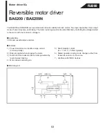
Page 45: ...PNP tr Additional OP amp built in Applications MD CD CD ROM drive DVD DVD ROM drive HSOP042 P 0400 Unit mm 1 7 8 14 1 315 0 65 0 20 28 22 21 4 8 6 4 1 2 5 15 18 4 0 2 8 3 0 2 2 7 0 2 0 1 0 1 10 93 0 30 15 0 35 0 10 0 05 0 30 0 10 0 05 0 8 Seating plane 0 to 10 Block Diagram 19 PGND1 20 PV CC1 23 IN1 18 VO1 24 PC1 17 VO1 25 IN2 16 VO2 26 PC2 15 VO2 27 IN3 14 VO3 13 VO3 28 IN4 12 VO4 10 PGND2 11 VO4...

Page 46: ...pin 6 Op amp non inverted input pin 7 Power supply pin 8 1 2 PVCC output pin 2 9 Driver power supply pin 2 10 Driver GND pin 2 11 Motor driver 4 reverse rotation output pin 12 Motor driver 4 forward rotation output pin 13 Motor driver 3 reverse rotation output pin 14 Motor driver 3 forward rotation output pin Parameter Symbol Range Unit Supply voltage SVCC PVCC1 PVCC2 4 0 to 14 V Recommended Opera...

Page 47: ... driver 1 High level threshold voltage VPCH1 VCC 5 V RL1 8 Ω R1 10 kΩ 2 0 V Low level threshold voltage VPCL1 VCC 5 V RL1 8 Ω R1 10 kΩ 0 5 V Motor driver 2 High level threshold voltage VPCH2 VCC 5 V RL2 8 Ω R2 10 kΩ 2 0 V Low level threshold voltage VPCL2 VCC 5 V RL2 8 Ω R2 10 kΩ 0 5 V Reset circuit Reset operation release supply VRST IIN 10 µA R1 to R 4 10 kΩ 2 1 2 3 2 5 V voltage 3 3 V regulator...

Page 48: ...not guaranteed Usage Notes 1 Avoid the short circuits between output and VCC and between output pin and GND Otherwise the IC is likely to break down or emit smoke 2 An appropriate prior study should be done for use of dip soldering Application Notes PD Ta curves of HSOP042 P 0400 PD Ta 0 000 0 25 50 75 100 125 150 2 500 1 500 1 000 2 240 2 000 1 042 0 500 Ambient temperature Ta C Power dissipation...

Page 49: ...re that im proves audio dynamic performance and reduces jitter sensitivity The internal digital filter operates at 8x oversampling at a 96kHz sampling rate with 120dB stopband attenuation International Airport Industrial Park Mailing Address PO Box 11400 Tucson AZ 85734 Street Address 6730 S Tucson Blvd Tucson AZ 85706 Tel 520 746 1111 Twx 910 952 1111 Internet http www burr brown com Cable BBRCOR...

Page 50: ...age 6 Full Scale 0dB 0 57 VCC Vp p Center Voltage 0 5 VCC V Load Impedance AC Load 5 kΩ DIGITAL FILTER PERFORMANCE Filter Characteristics 1 fS 44 1kHz 48kHz optimal Passband 0 002dB 0 471fS 3dB 0 487fS Stopband 0 515fS Passband Ripple 0 453fS 0 0001 dB Stopband Attenuation Stopband 0 515fS 109 dB Stopband 0 520fS 123 dB Delay Time 81 fS sec Filter Characteristics 2 fS 88 2kHz 96kHz optimal Passban...

Page 51: ...38 dB Dynamic Range EIAJ A Weighted 4 104 dB Output Voltage Sine Wave 0dBFS Without Peak Extend 2 0 57VCC Vp p 0dBFS With Peak Extend 5 0 285VCC Vp p 6dBFS 5 6 0 57VCC Vp p DYNAMIC ANALOG PERFORMANCE Standard CD Digital HDCD SCALING 1 Total Harmonic Distortion Noise VO 0dB 0dBFS 92 dB VO 60dB 33 dB Dynamic Range EIAJ A Weighted 96 dB Output Voltage Sine Wave 0dBFS 0 285VCC Vp p DYNAMIC ANALOG PERF...

Page 52: ...s integrated circuit can be damaged by ESD Burr Brown recommends that all integrated circuits be handled with appropriate precautions Failure to observe proper handling and installation procedures can cause damage ESD damage can range from subtle performance degradation to complete device failure Precision integrated circuits may be more susceptible to damage because very small parametric changes ...

Page 53: ... motor with the control pin voltage VR Applications VCRs and cassette tape recorders Features 1 Power transistors can handle a large current 1 6A maximally 2 Brake is applied when stopping the motor 3 Built in function to absorb rush currents generated by reversing and braking 4 Motor speed controlling pin 5 Small standby current VCC 12V IO 5 5mA typically 6 Stable operation during mode changes ei...

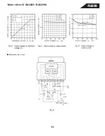
Page 54: ...Motor driver IC BA6209 BA6209N Measurement circuit FL8380 54 ...

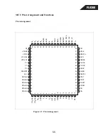
Page 55: ...OCK TLOCK SQCK SUBQ DMUTE STAT XRST PUSW CDRW P61 P60 32 31 30 29 28 27 26 25 24 23 22 21 20 19 18 17 P2 1 P2 0 P8 7 P8 6 AMUTE HDCD RL RL TRSW DSNS POWER DACRST DAC DATA DAC CLK DAC LD V CC PB 1 AN 1 PB 0 AN 0 AV SS TEST X 2 X 1 V SS OSC 1 OSC 2 RES S0 S1 S2 DN UP S0S1 P22 VFD DO VFD DI VFD CLK VFD LAT P14 P1 5 P16 REMOTE AVCC PB7 AN7 PB6 AN6 PB5 AN5 PB4 AN4 PB3 AN3 PB2 AN2 Figure 1 2 Pin Arrange...

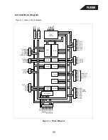
Page 56: ...1 P50 INT0 Port 1 P10 TMOW P14 PWM P15 IRQ1 P16 IRQ2 P17 IRQ3 TRGV Port 2 P20 SCK3 P21 RXD P22 TXD Port 3 P30 SCK1 P31 SI1 P32 SO1 P90 FVPP P91 P92 P93 P94 Port 9 PB 0 AN 0 PB 1 AN 1 PB 2 AN 2 PB 3 AN 3 PB 4 AN 4 PB 5 AN 5 PB 6 AN 6 PB 7 AN 7 V SS V CC RES IRQ 0 TEST OSC 1 OSC 2 X 1 X 2 CPU H8 300L Data bus lower System clock generator Subclock generator RAM Timer A SCI1 Timer B1 Watchdog timer A ...

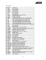
Page 57: ...pickup at inner position 21 XRST CD DSP reset line 0V DSP reset 22 STAT CD DSP internal status output 23 DMUTE CD DSP mute control 5V mute on 24 SUBQ SUBQ output 25 SQCK SUBQ output serial clock 26 TLOCK No connection 27 FLOCK No connection 28 SENSE No connection 29 MLD CD DSP command latch 30 MDATA CD DSP serial command data 31 MCLK CD DSP serial command clock 32 P57 No connection 33 VCC MCU powe...

Page 58: ... VFD CLK Display driver command serial clock 53 VFD LAT Display driver command serial latch 54 P14 No connection 55 P15 No connection 56 P16 CD DSP internal status for auto adjustment 57 REMOTE IR remote signal input 58 AVCC Connected to 5V 59 PB7 No connection 60 PB6 No connection 61 PB5 No connection 62 PB4 No connection 63 PB3 No connection 64 PB2 No connection FL8380 58 ...

Page 59: ...FL8380 59 ...

Page 60: ...FL8380 60 ...

Page 61: ...BON FILM RESISTOR 4 7K OHM 1 6W 5 TP52 3 R32 R33 R38 1004 703316 020 CARBON FILM RESISTOR 47K OHM 1 6W 5 TP52 3 R116 1005 100316 020 CARBON FILM RESISTOR 51 OHM 1 6W 5 AXIAL TAPE 1 R36 1005 102316 020 CARBON FILM RESISTOR 5 1K OHM 1 6W 5 AXIAL TAPE 1 R56 R57 1005 602316 020 CARBON FILM RESISTOR 5 6K OHM 1 6W 5 TP52 2 R67 1005 603316 020 CARBON FILM RESISTOR 56K OHM 1 6W 5 TP52 1 R73 1006 802316 02...

Page 62: ...O 92 SAMSUNG 1 DIODE ZENER BRIDGE IC7 IC8 1401 101000 000 BRIDGE RECTIFIER DB101 50V 1A UL 2 D10 D11 1401 113300 000 DIODE 1SS133 ROHM 2 D2 D3 D4 D5 1401 140040 000 DIODE RECTIFIER 1N4004 4 D1 D6 D9 D12 D13 1401 141480 000 DIODE 1N4148 5 D7 1402 240001 200 ZENER DIODE DZ24V 1 D8 1402 471201 200 ZENER DIODE 4 7V 1 2W 1 Z1 1402 620001 200 ZENER DIODE 6 2V 1 2W 1 Z2 1402 620001 200 ZENER DIODE 6 2V 1...

Page 63: ...03044 000 CERAMIC CAP 0 01UF 50V 20 2 C407 C408 1101 473062 000 POLYESTER MYLAR CAP 0 047UF 100V 5 2 C409 C411 1102 101024 000 ELECT CAP 100UF 25V 20 2 C401 1102 471014 000 ELECT CAP 470uF 16V 20 8X12MM 1 CONNECTOR CN401 2300 006000 000 STRAIGHT CONN WAFER 6 PINS 2mmP 1 JK401 2320 009911 003 6 4MM HEADPHONE JACK JY 6303 02 030 GOLD PLATED 1 IC IC401 4145 600001 600 I C NJM4560L 8PINS SIL NJRC 1 66...

Page 64: ...0 362000 000 LASER PICK UP LABEL 1 6029 010012 001 01 PLASTIC FOOT HOT STAMPING 4 6083 510011 000 STAND FRONT 5CD 1 6083 510012 000 STAND REAR 5CD 1 6083 510013 001 BRACKET 5CD SIDE 1 1 6083 510014 001 BRACKET 5CD SIDE 2 1 6083 510016 000 BRACKET WIRE 1 6083 810002 000 01 HARMAN KARDON FL8380 CD TRAY DOOR W SILKSCREEN 1 6083 810003 001 01 HARMAN KARDON FL8380 DISPLAY LENS W SILKSCREEN 1 6083 81001...

Page 65: ...000 PHOTO COUPLER SG206 OPTO SENSOR 1 D3 3100 800000 000 EMITTING DIODE EL 8L OPTO SENSOR 1 PCB MISC 4841 010130 003 5CD SENSOR BD REV C 1 6005 050029 001 HOLDER SENSOR 1 6005 050032 000 COVER HOLDER SENSOR 1 5CD CHANGER MECHANICAL ASSY 2501 062801 150 6PIN 280MM 2CONN RIBBON CABLE AWG 28 2MMP 1 6505 050002 001 CABINET HOLDER A 4 7003 008002 112 SCREW M3X8 P T P B H 4 8500 055080 300 CABINET TOP A...

Page 66: ... 008002 112 SCREW M3X8 P T P B H 8 7003 008003 112 SCREW M3X8 B TYPE B H ZN 1 7003 012002 062 SCREW M3X12 P T P W H 1 7103 207004 000 FIBRE WASHER M3 2X7X0 4MM 1 7103 209008 022 WASHER M3 2X9X0 8 3 7103 210012 022 PLAN WASHER 3 2X10X1 2t ZN 2 7103 314010 022 WASHER M3 3X14X1MM ST ZN 1 7105 010005 030 WASHER LOCK 5X10X0 5MM 3 7106 212505 022 PLAN WASHER 6 2X12 5X0 5t 3 8500 055010 100 BRACKET GEAR ...

Page 67: ...URN TABLE BOARD ASSY REV A 2300 002000 001 STRAIGHT CONN WAFER 2PIN 2MMP JST 1 2300 006000 000 STRAIGHT CONN WAFER 6 PINS 2mmP 1 2501 062801 150 6PIN 280MM 2CONN RIBBON CABLE AWG 28 2MMP 1 4841 010700 006 5CD TURN TABLE REV F 1 67 ...

Page 68: ...FL8380 68 ...

Page 69: ...FL8380 69 ...

Page 70: ...FL8380 70 ...

Page 71: ...FL8380 71 ...

Page 72: ...1 10 Outer Carton 1 2 5000 835001 001 End Packing Foam 2 3 FL 8380 FL8380 Unit 1 4 9805 020000 071 FL8380 Remote Control 1 5 2617 210004 001 Cable 1 6 2611 310009 000 RCA Cable 1 7 Warranty Sheet 1 8 Instruction Sheet 1 9 5100 838000 000 Owner s Manual 1 72 ...

Reviews: