
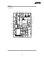
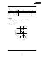
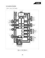
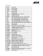


FL8380
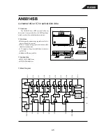
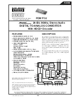
PCM1732
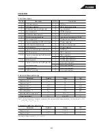
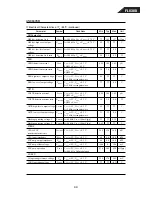
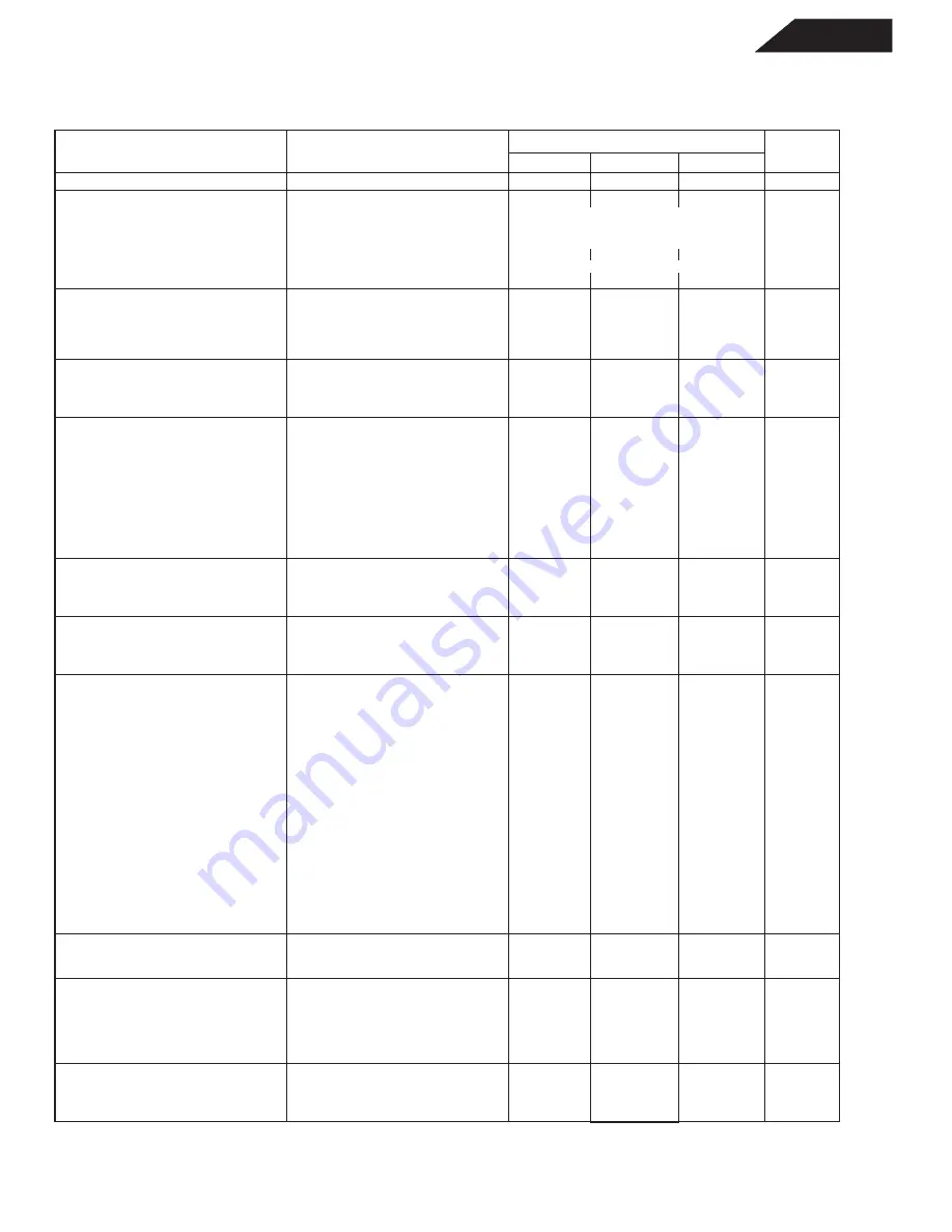
SPECIFICATIONS
24-Bit Data Performance
All specifications at +25
°
C, +V
CC
= +V
DD
= +5V, f
S
= 44.1kHz, and SYSCLK = 384f
S
, unless otherwise noted.
PCM1732
PARAMETER
CONDITIONS
MIN
TYP
MAX
UNITS
RESOLUTION
24
Bits
DATA FORMAT
Audio Data Interface Format
Standard/I
2
S
Data Bit Length
16/20/24 Selectable
Audio Data Format
MSB-First, Binary Two’s Complement
Sampling Frequency (f
S
)
16
96
kHz
System Clock Frequency
(1)
256/384/512/768f
S
System Clock Duty Cycle
40
60
%
DIGITAL INPUT/OUTPUT LOGIC LEVEL
Input Logic Level (except XTI): V
IH
2.0
V
V
IL
0.8
V
Output Logic Level (CLKO):
V
OH
I
OH
= 2mA
4.5
V
V
OL
I
OL
= 4mA
0.5
V
CLKO PERFORMANCE
(2)
Output Rise Time
20 ~ 80% V
DD
, 10pF
5.5
ns
Output Fall Time
80 ~ 20% V
DD
, 10pF
4
ns
Output Duty Cycle
10pF Load
30
%
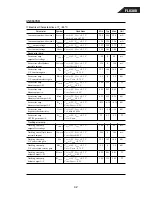
DYNAMIC PERFORMANCE
(3, 4)
THD+N
V
O
= 0dB
f
S
= 44.1kHz
–96
–90
dB
f
S
= 96kHz
–94
dB
V
O
= –60dB
f
S
= 44.1kHz
–42
dB
Dynamic Range
f
S
= 44.1kHz, EIAJ A-weighted
98
104
dB
f
S
= 96kHz, A-weighted
103
dB
Signal-to-Noise Ratio
(5)
f
S
= 44.1kHz, EIAJ A-weighted
98
104
dB
f
S
= 96kHz, A-weighted
103
dB
Channel Separation
f
S
= 44.1kHz
96
104
dB
f
S
= 96kHz
101
dB
DC ACCURACY
Gain Error
±
1.0
±
3.0
% of FSR
Gain Mismatch Channel-to-Channel
±
1.0
±
3.0
% of FSR
Bipolar Zero Error
V
O
= 0.5V
CC
at Bipolar Zero
±
30
±
60
mV
ANALOG OUTPUT
Output Voltage
(6)
Full Scale (0dB)
0.57 V
CC
Vp-p
Center Voltage
0.5 V
CC
V
Load Impedance
AC Load
5
k
Ω
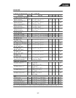
DIGITAL FILTER PERFORMANCE
Filter Characteristics 1
(f
S
= 44.1kHz/48kHz optimal)
Passband
±
0.002dB
0.471f
S
–3dB
0.487f
S
Stopband
0.515f
S
Passband Ripple
< 0.453f
S
±
0.0001
dB
Stopband Attenuation
Stopband = 0.515f
S
–109
dB
Stopband = 0.520f
S
–123
dB
Delay Time
81/f
S
sec
Filter Characteristics 2
(f
S
= 88.2kHz/96kHz optimal)
Passband
±
0.005dB
0.395f
S
–3dB
0.441f
S
Stopband
0.538f
S
Passband Ripple
< 0.341f
S
±
0.0001
dB
Stopband Attenuation
Stopband = 0.538f
S
–132
dB
Delay Time
31/f
S
sec
De-Emphasis Error
±
0.1
dB
INTERNAL ANALOG FILTER
–3dB Bandwidth
100
kHz
Passband Response
f = 20kHz
–0.16
dB
POWER SUPPLY REQUIREMENTS
Voltage Range
V
DD,
V
CC
4.5
5
5.5
VDC
Supply Current: I
CC
+ I
DD
f
S
= 44.1kHz
35
105
mA
f
S
= 96kHz
93
mA
Power Dissipation
f
S
= 44.1kHz
425
525
mW
f
S
= 96kHz
465
mW
TEMPERATURE RANGE
Operating
–25
+70
°
C
Storage
–55
+100
°
C
Thermal Resistance,
θ
JA
67
°
C/W
NOTES: (1) Refer to the System Clock section of this data sheet. (2) An external buffer is recommended. (3) Dynamic performance specifications are tested with 20kHz low-pass
filter and THD+N specifications are tested with 30kHz LPF, 400Hz HPF, Average Mode. (4) Dynamic performance specifications are tested with HDCD gain scaling set to analog
gain scaling. (5) SNR is tested with infinite zero detection off. (6) Output level is for sine wave. DAC outputs 0.64 V
CC
(peak-to-peak) due to filter response as transient.
50
Summary of Contents for FL 8380
Page 21: ...FL8380 ...
Page 22: ...FL8380 ...
Page 23: ...FL8380 ...
Page 24: ...FL8380 ...
Page 25: ...FL8380 ...
Page 27: ...FL8380 27 ...
Page 28: ...FL8380 28 ...
Page 29: ...FL8380 29 ...
Page 30: ...FL8380 30 ...
Page 31: ...FL8380 31 ...
Page 32: ...FL8380 32 ...
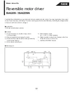
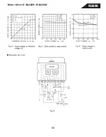
Page 54: ...Motor driver IC BA6209 BA6209N Measurement circuit FL8380 54 ...
Page 59: ...FL8380 59 ...
Page 60: ...FL8380 60 ...
Page 68: ...FL8380 68 ...
Page 69: ...FL8380 69 ...
Page 70: ...FL8380 70 ...
Page 71: ...FL8380 71 ...