


18
Subject to change without notice
Testing Semiconductors
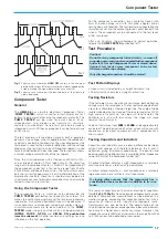
Most semiconductor devices, such as diodes, Z-diodes,
transistors, FETs can be tested. The test pattern displays vary
according to the component type as shown in the figures
below.
The main characteristic displayed during semiconductor testing
is the voltage dependent knee caused by the junction changing
from the conducting state to the non conducting state. It
should be noted that both the forward and the reverse
characteristic are displayed simultaneously. This is a two-
terminal test, therefore testing of transistor amplification is
not possible, but testing of a single junction is easily and
quickly possible. Since the test voltage applied is only very
low, all sections of most semiconductors can be tested
without damage. However, checking the breakdown or reverse
voltage of high voltage semiconductors is not possible. More
important is testing components for open or short-circuit,
which from experience is most frequently needed.
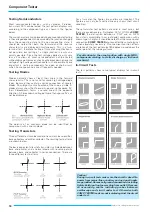
Testing Diodes
Diodes normally show at least their knee in the forward
characteristic. This is not valid for some high voltage diode
types, because they contain a series connection of several
diodes. Possibly only a small portion of the knee is visible. Z-
diodes always show their forward knee and, up to approx. 9V,
their Z-breakdown, forms a second knee in the opposite
direction. A Z-breakdown voltage of more than approx. 9V can
not be displayed.
The polarity of an unknown diode can be identified by
comparison with a known diode.
Testing Transistors
Three different tests can be made to transistors: base-emitter,
base-collector and emitter-collector. The resulting test patterns
are shown below.
The basic equivalent circuit of a transistor is a Z-diode between
base and emitter and a normal diode with reverse polarity
between base and collector in series connection. There are
three different test patterns:
For a transistor the figures b-e and b-c are important. The
figure e-c can vary; but a vertical line only shows short circuit
condition.
These transistor test patterns are valid in most cases, but
there are exceptions (e.g. Darlington, FETs). With the
COMP.
TESTER
, the distinction between a P-N-P and an N-P-N
transistor is discernible. In case of doubt, comparison with a
known type is helpful. It should be noted that the same socket
connection (
COMP. TESTER
or ground) for the same terminal
is then absolutely necessary. A connection inversion effects
a rotation of the test pattern by 180 degrees round about the
center point of the scope graticule.
Pay attention to the usual caution with single MOS-
components relating to static discharge or frictional
electricity!
In-Circuit Tests
The test patterns show some typical displays for in-circuit
tests.
Caution!
During in-circuit tests make sure the circuit is dead. No
power from mains/line or battery and no signal inputs
are permitted. Remove all ground connections including
Safety Earth (pull out power plug from outlet). Remove
all measuring cables including probes between
oscilloscope and circuit under test. Otherwise both
COMP. TESTER leads are not isolated against the circuit
under test.
Component Tester


