Model L3149B C200 Advanced Desk Set
Foreword
3
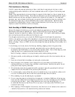
FCC Interference Warning
The FCC requires that manuals pertaining to Class A and Class B computing devices must contain
warnings about possible interference with local residential radio and TV reception. This warning reads
as follows:
N
OTE
:
This equipment has been tested and found to comply with the limits for a Class A digital device,
pursuant to Part 15 of the FCC Rules. These limits are designed to provide reasonable protection against
harmful interference when the equipment is operated in a commercial environment. This equipment
generates, uses, and can radiate radio frequency energy and, if not installed and used in accordance with
the instruction manual, may cause harmful interference to radio communications. Operation of this
equipment in a residential area is likely to cause harmful interference in which case the user will be
required to correct the interference at his own expense.
Safe Handling of CMOS Integrated Circuit Devices
Many of the integrated circuit devices used in communications equipment are of the Complementary
Metal Oxide Semiconductor (CMOS) type. Because of their high open circuit impedance, CMOS
integrated circuits are vulnerable to damage from static charges. Care must be taken handling, shipping,
and servicing them and the assemblies in which they are used.
Even though protection devices are provided in CMOS integrated circuit inputs, the protection is
effective only against over-voltage in the hundreds of volts range such as is encountered in an operating
system. In a system, circuit elements distribute static charges and load the CMOS circuits, decreasing the
chance of damage. However, CMOS circuits can be damaged by improper handling of the modules, even
in a system.
To avoid damage to circuits, observe the following handling, shipping, and servicing precautions:
1.
Prior to and while servicing a circuit module, particularly after moving within the service area,
momentarily touch both hands to a bare metal, earth-grounded surface. This will discharge any static
charge that may have accumulated on the person doing the servicing.
N
OTE
:
Wearing a conductive wrist strap minimizes static build-up during servicing.
2.
Whenever possible, avoid touching any electrically conductive parts of the circuit module with your
hands.
3.
Power down the unit before installing or removing the circuit module.
4.
When servicing a circuit module, avoid carpeted areas, dry environments, and certain types of
clothing (silk, nylon, etc.) because they contribute to static build-up. Similarly, disconnect the test
probe prior to removing the ground lead.
5.
All electrically powered test equipment should be grounded. Apply the ground lead from the test
equipment to the circuit module before connecting the test probe.
6.
If a circuit module is removed from the system, it is desirable to lay it on a conductive surface (such
as a sheet of aluminum foil) that is connected to ground through 100k of resistance.
7.
When soldering, be sure the soldering iron is grounded.
8.
Prior to connecting jumpers, replacing circuit components, or touching CMOS pins (if this becomes
necessary in the replacement of an integrated circuit device), be sure to discharge any static build-up
as described in procedure 1. Since voltage differences can exist across the human body, it is
recommended that only one hand be used if it is necessary to touch pins on the CMOS device and
associated board wiring.
9.
When replacing a CMOS integrated circuit device, leave the device in its conductive rail container or
conductive foam until it is to be inserted into the printed circuit module.
Summary of Contents for L3149B
Page 77: ...71 Schematics ...
Page 78: ...Schematics Model L3149B C200 Advanced Desk Set 72 DeskSetLineInterfaceSchematicDiagram Sheet1 ...
Page 79: ...Model L3149B C200 Advanced Desk Set Schematics 73 DeskSetUserAudioI OSchematicDiagram Sheet2 ...
Page 81: ...Model L3149B C200 Advanced Desk Set Schematics 75 DeskSetDSPBlockSchematicDiagram Sheet4 ...
Page 82: ...Schematics Model L3149B C200 Advanced Desk Set 76 DeskSetToneKeypanelSchematicDiagram Sheet5 ...
Page 83: ...Model L3149B C200 Advanced Desk Set Schematics 77 DeskSetPowerSupplySchematicDiagram Sheet6 ...
Page 85: ...Model L3149B C200 Advanced Desk Set Schematics 79 RelayI OOptionSchematicDiagram XRC0001A ...
Page 86: ...Schematics Model L3149B C200 Advanced Desk Set 80 NOTES ...
Page 87: ...81 Circuit Boards ...
Page 88: ...Circuit Boards Model L3149B C200 Advanced Desk Set 82 MainUnitDTDCircuitBoard ...
Page 89: ...Model L3149B C200 Advanced Desk Set Circuit Boards 83 MainUnitPowerandLineCircuitBoard ...
Page 90: ...Circuit Boards Model L3149B C200 Advanced Desk Set 84 RelayI OOptionCircuitBoard ...
Page 92: ...Notes Model L3149B C200 Advanced Desk Set 86 ...


