background image

3-1-3

HC4S4PEX

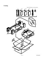
Some Ref. Numbers are not in sequence.

X2

X20C

X3

X20B

X20A

X1

X4

S1

Unit

S3

S2

S2

A14


Packing

Summary of Contents for 25A-664

Page 1: ...rvicing I Adjustment Procedures I Schematic Diagrams I CBA s Sec 2 Deck Mechanism Section I Standard Maintenance I Alignment for Mechanism I Disassembly Assembly of Mechanism I Alignment Procedures of Mechanism Sec 3 Exploded views and Parts List Section I Exploded views I Parts List 25A 664 PAL ...

Page 2: ... Disassembly Instructions 1 5 1 Electrical Adjustment Instructions 1 6 1 Block Diagrams 1 7 1 Function Indicator Symbols 1 7 11 Schematic Diagrams CBA s and Test Points 1 8 1 Waveforms 1 9 1 Wiring Diagrams 1 10 1 IC Pin Function Descriptions 1 11 1 Lead Identifications 1 12 1 Sec 1 Main Section I Specifications I Preparation for Servicing I Adjustment Procedures I Schematic Diagrams I CBA s ...

Page 3: ...urst 1 4 Video Color S N AM R P dB 37 41 SP Mode 1 5 Video Color S N PM R P dB 30 36 SP Mode 1 6 Resolution PB Line 230 245 SP Mode 2 Servo 2 1 Jitter Low µsec 0 07 0 12 SP Mode 2 2 Wow Flutter 0 3 0 5 SP Mode 3 Normal Audio 3 1 Output PB dBV 9 6 3 SP Mode 3 2 Output R P dBV 9 6 1 5 SP Mode 3 3 S N R P dB 36 41 SP Mode 3 4 Distortion R P 1 0 4 0 SP Mode 3 5 Freq resp R P at 200Hz dB 7 4 SP Mode 20...

Page 4: ...especially 1 Wires covered with PVC tubing 2 Double insulated wires 3 High voltage leads D Use specified insulating materials for hazardous live parts Note especially 1 Insulation tape 2 PVC tubing 3 Spacers 4 Insulators for transistors E When replacing AC primary side components transformers power cord etc wrap ends of wires securely about the terminals before solder ing F Observe that the wires ...

Page 5: ...arts RF termi nals antenna terminals video and audio input and output terminals microphone jacks earphone jacks etc is lower than or equal to the specified value in the table below Measuring Method Power ON Insert load Z between B earth ground power cord plug prongs and exposed accessible parts Use an AC voltmeter to measure across the terminals of load Z See Fig 2 and the following table AC Line ...

Page 6: ...e the flat pack IC with tweezers while apply ing the hot air 3 Bottom of the flat pack IC is fixed with glue to the CBA when removing entire flat pack IC first apply soldering iron to center of the flat pack IC and heat up Then remove glue will be melted Fig S 1 6 4 Release the flat pack IC from the CBA using twee zers Fig S 1 6 Caution 1 Do not supply hot air to the chip parts around the flat pac...

Page 7: ... pins of the flat pack IC you can remove it easily Fig S 1 3 2 Affix the wire to a workbench or solid mounting point as shown in Fig S 1 5 3 While heating the pins using a fine tip soldering iron or hot air blower pull up the wire as the solder melts so as to lift the IC leads from the CBA contact pads as shown in Fig S 1 5 4 Bottom of the flat pack IC is fixed with glue to the CBA when removing e...

Page 8: ...ur due to a potential difference caused by electro static charge during unpacking or repair work 1 Ground for Human Body Be sure to wear a grounding band 1MΩ that is prop erly grounded to remove any static electricity that may be charged on the body 2 Ground for Workbench Be sure to place a conductive sheet or copper plate with proper grounding 1MΩ on the workbench or other surface where the semi ...

Page 9: ...s will stop the function of Tape Start Sensor Tape End Sen sor and Reel Sensors If these TPs are connected before plugging in the unit the function of the sensors will stay valid See Fig 1 Note Because the Tape End Sensors are inactive do not run a tape all the way to the start or the end of the tape to avoid tape damage About REC Safety Switch Caution The REC Safety Switch is directly mounted on ...

Page 10: ...e Be careful not to break them 1 Release Locking Tab L 3 and remove Screw S 2 five Screws S 3 three Screws S 4 and Screw S 5 Then slowly lift the VCR Chassis Unit Deck Assembly Function CBA Jack CBA and Main CBA up 2 When reassembling solder wire jumpers as shown in Fig 5 3 Before installing the Deck Assembly be sure to place the pin of LD SW on Main CBA as shown in Fig 6 Then install the Deck Ass...

Page 11: ...1 5 2 HC2C0DC S 1 S 1 S 1 1 Top Case Fig 1 L 2 L 1 2 Front Assembly L 2 Fig 2 S 4 S 3 S 3 S 3 S 4 3 VCR Chassis Unit L 3 S 5 Fig 3 S 6 4 Jack CBA Desolder Fig 4 ...

Page 12: ... Assembly TOP VIEW From FE Head From Cylinder Assembly From AC Head Assembly Lead with red stripe Lead with white stripe Lead with white stripe From Capstan Motor Assembly Lead connections of Deck Assembly and Main CBA Fig 5 LD SW Pin Hole Hole Shaft Cam Gear 7 Main CBA 6 Deck Assembly 7 Main CBA SW507 LD SW Pin Fig 6 ...

Page 13: ...scope Dual trace with 10 1 probe V Range 0 001 50V Div F Range DC AC 20MHz 2 Alignment Tape FL6A Head Switching Position Adjustment Purpose To determine the Head Switching point during playback Symptom of Misadjustment May cause Head Switching noise or vertical jitter in the picture Reference Notes Playback the Alignment tape and adjust VR501 so that the V sync front edge of the CH1 video output w...

Page 14: ...L 67 66 86 P DOWN L C SYNC 58 SW506 TO VIDEO BLOCK TO Hi Fi AUDIO BLOCK TO AUDIO BLOCK 2 2 KEY 2 4 4 KEY 1 KEY SWITCH KEY SWITCH CL505 CN651 FUNCTION CBA 1 7 1 1 7 2 HC4S4BLS SDA SDA SCL SCL TU701 TUNER UNIT IC503 MEMORY 72 61 19 83 IIC BUS SCL D V SYNC D REC H DAVN L RF SW H A SW C ROTA IIC BUS SDA H A COMP V ENV C SYNC IIC BUS SCL 71 3 5 SDA SCL 12 11 LD SW 9 AL 15V 12V AL 12V AL 5V AL 5V SW507 ...

Page 15: ... DECORDER V OUT1 1 V IN1 1 3 3 V OUT2 1 V IN2 3 1 3 JACK CBA 48 50 52 56 24 6 50 52 19 20 JK101 V OUT1 V IN1 19 20 JK102 CL151 CL152 CL101 CL102 V OUT2 V IN2 61 63 96 95 93 94 90 89 88 87 CHARA INS CCD 1H DELAY SP BYPASS MUTE PB EE IN1 TUNER IN1 TUNER MUTE PB EE FRT IN2 FRT IN2 AGC P R R Y C P R P R P EP Y DELAY Y C MIX 21 79 78 AGC VXO OSD CHARACTER MIX FBC 1 2 58 59 65 29 28 IIC BUS SDA 69 68 46...

Page 16: ... P TUNER IN2 IN1 R ALC DET ALC IC301 AUDIO SIGNAL PROCESS 15 13 17 4 A PB REC CL504 3 A COM 1 AE H 2 AE H FE H A PB REC 4 A COM 3 AE H 1 AE H FE H 2 CL287 AUDIO HEAD AUDIO ERASE HEAD ACE HEAD ASSEMBLY FE HEAD 2 FE H 1 FE H GND CL501 1 7 5 1 7 6 HC4S4BLA MAIN CBA PB AUDIO SIGNAL REC AUDIO SIGNAL Mode SP REC 71 A MUTE H IIC BUS SCL IIC BUS SDA TO SERVO SYSTEM CONTROL BLOCK FULL ERASE HEAD 68 69 SERI...

Page 17: ... R HEAD Hi Fi AUDIO L HEAD CYLINDER ASSEMBLY MAIN CBA Hi Fi A R 7 Hi Fi COM 8 Hi Fi A L 9 CL253 IC451 MTS SAP Hi Fi AUDIO PROCESS Hi Fi HEAD AMP Hi Fi Audio Block Diagram HC4S4BLH REC AUDIO SIGNAL PB AUDIO SIGNAL Mode SP REC JACK CBA AFV CBA JK101 A IN1 R A IN1 L 2 6 2 6 1 3 1 3 JK102 CL151 CL152 CL101 CL102 A IN2 R A IN2 L A OUT1 R A OUT1 L A OUT2 R A OUT2 L TU AUDIO R 4 TU AUDIO L 5 4 5 CN701 CN...

Page 18: ...eck to see that all components in the power supply circuit are not defective before you connect the AC plug to the AC power supply Otherwise it may cause some components in the power supply circuit to fail HC4S4BLP 1 7 9 1 7 10 COLD MAIN CBA HOT CIRCUIT BE CAREFUL HOT IC001 ERROR VOLTAGE DET Q002 Q003 Q001 F001 L003 LINE FILTER BRIDGE RECTIFIER D001 D004 1 2 3 4 Q004 SHUNT REGULATOR REG AC001 T001...

Page 19: ... 88 88 ON POWER ON PWR ON REC REC ON REC PAUSE REC Blinks at 0 8Hz interval T REC OTR ON T REC OFF T REC incomplete Blinks at 0 8Hz interval When reel and capstan mechanism is not functioning correctly 1 Blinks at 0 8Hz interval When tape loading mechanism is not func tioning correctly 2 Blinks at 0 8Hz interval When cassette loading mechanism is not functioning correctly 3 Blinks at 0 8Hz interva...

Page 20: ...fully The use of substitute replacement parts that do not have the same safety characteristics as speci fied in the parts list may create shock fire or other hazards Capacitor Temperature Markings Notes 1 Do not use the part number shown on these draw ings for ordering The correct part number is shown in the parts list and may be slightly different or amended since these drawings were prepared 2 A...

Page 21: ...e only original replacement parts which are listed with their part numbers in the parts list section of the service manual 4 Wire Connectors 1 Prefix symbol CN means connector can disconnect and reconnect 2 Prefix symbol CL means wire solder holes of the PCB wire is soldered directly 5 Mode SP REC 6 Voltage indications for PLAY and REC modes on the schematics are as shown below 7 How to read conve...

Page 22: ...1 8 3 1 8 4 1 8 5 HC4S4SCM1 Main 1 5 Schematic Diagram ...

Page 23: ...1 8 6 1 8 7 1 8 8 HC4S4SCM2 Main 2 5 Schematic Diagram ...

Page 24: ...1 8 9 1 8 10 1 8 11 HC4S4SCM3 Main 3 5 Schematic Diagram ...

Page 25: ...AGAINST FIRE HAZARD REPLACE ONLY WITH THE SAME TYPE FUSE CAUTION Fixed voltage or Auto voltage selectable power supply circuit is used in this unit If Main Fuse F001 is blown check to see that all components in the power supply circuit are not defective before you connect the AC plug to the AC power supply Otherwise it may cause some components in the power supply circuit to fail ...

Page 26: ...Main 5 5 Schematic Diagram 1 8 15 1 8 16 HC4S4SCM5 ...

Page 27: ...VPS Schematic Diagram 1 8 17 1 8 18 HC4S4SCV ...

Page 28: ...1 8 19 1 8 20 HC4S4SCF Function Schematic Diagram ...

Page 29: ...AFV Schematic Diagram 1 8 21 1 8 22 HC4S4SCAFV ...

Page 30: ...Jack Schematic Diagram 1 8 23 1 8 24 HC4S4SCJ ...

Page 31: ...1 8 25 1 8 26 Function CBA Top View Function CBA Bottom View BHC400F01018 B ...

Page 32: ...1 8 27 1 8 28 AFV CBA Top View AFV CBA Bottom View BHC400F01091 VPS CBA Top View VPS CBA Bottom View BHC400F01018 C ...

Page 33: ...1 8 29 1 8 30 Jack CBA Top View Jack CBA Bottom View BHC400F01018 E ...

Page 34: ...ore you connect the AC plug to the AC power supply Otherwise it may cause some components in the power supply circuit to fail BECAUSE A HOT CHASSIS GROUND IS PRESENT IN THE POWER SUPPLY CIRCUIT AN ISOLATION TRANSFORMER MUST BE USED ALSO IN ORDER TO HAVE THE ABILITY TO INCREASE THE INPUT SLOWLY WHEN TROUBLESHOOTING THIS TYPE POWER SUPPLY CIRCUIT A VARIABLE ISOLATION TRANSFORMER IS REQUIRED NOTE The...

Page 35: ...ause some components in the power supply circuit to fail BECAUSE A HOT CHASSIS GROUND IS PRESENT IN THE POWER SUPPLY CIRCUIT AN ISOLATION TRANSFORMER MUST BE USED ALSO IN ORDER TO HAVE THE ABILITY TO INCREASE THE INPUT SLOWLY WHEN TROUBLESHOOTING THIS TYPE POWER SUPPLY CIRCUIT A VARIABLE ISOLATION TRANSFORMER IS REQUIRED NOTE The voltage for parts in hot circuit is measured using hot GND as a comm...

Page 36: ...0usec 50mV x 10 WAVEFORMS TP751 of Main CBA WF1 UPPER WF2 LOWER V OUT 0 1V x 10 RF SW 0 5V x 10 50usec TP751 of Main CBA TP302 of Main CBA WF5 C PB 10mV x 10 RF SW 0 5V x 10 5msec UPPER LOWER WF2 TP302 of Main CBA TP301 of Main CBA ...

Page 37: ...E IS SOLDERED DIRECTLY AC HEAD ASSEMBLY AUDIO HEAD AUDIO ERASE HEAD CONTROL HEAD AE H AE H FE H A COM A PB REC CTL CTL 6 5 4 3 2 1 CL287 M LOADING MOTOR CYLINDER ASSEMBLY AE H 1 AE H FE H 2 A COM 3 A PB REC 4 CTL 5 CTL 6 Hi Fi A R 7 Hi Fi COM 8 Hi Fi A L 9 V COM 5 V R 2 6 V R 1 1 V COM 2 V L 2 3 V L 1 4 AL 15V 12V 12 C F R 11 P ON 5V 10 AL 12V 9 GND 8 C FG 7 C CONT 6 GND 5 D FG 4 LM FWD REV 3 D CO...

Page 38: ...or Signal H L 18 OUT RF SW Video Head Switching Pulse H L 19 OUT HiFi H SW HiFi Audio Head Switching Pulse H L 20 IN DAVN L VPS PDC Data Receive L L 21 N U Not Used 22 OUT TUN SW2 Tuner System Control Signal Output H L 23 N U Not Used 24 N U Not Used 25 N U Not Used 26 N U Not Used 27 N U Not Used 28 N U Not Used 29 N U Not Used 30 N U Not Used 31 IN REC SAF SW Recording Safety SW Detect With Reco...

Page 39: ...um Motor Control Signal PWM 78 OUT C F R Capstan Motor FWD REV Control Signal FWD L REV H H L 79 IN S REEL Supply Reel Rotation Signal PULSE 80 IN T REEL Take Up Reel Rotation Signal PULSE 81 OUT LM FWD REV Loading Motor Control Signal H L Hi z 82 N U Not Used 83 OUT A MUTE H Audio Mute Control Signal Mute H H Pin No IN OUT Signal Name Function Active Level 84 OUT FF REW L CTL Amp Gain Switching S...

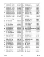
Page 40: ...GR BL 2SC2785 J H F K KRA103M KRC103M KRA104M 2SD1246 S T BN1L4M T KTA1281 Y 2SC1815 Y TPE2 2SC1815 GR TPE2 2SC3266 Y TPE2 2SC2120 Y TPE2 KTC3203 Y 2SC1815 BL TPE2 2SA1020 Y 2SB892 S KTC3205 Y 2SA1015 GR TPE2 E C B E C PT204 6B 12 MID 32A22 5 4 8 1 BR24C04F W AT24C04N 10SC M24C04 MN6 CAT24WC02JI PT 6958 FN TP 60 LA72646SM A MPB LC74793JM TRM 21 40 41 20 1 80 61 33 MSP3417G QG B8 V3 MSP3417G QG B8 ...

Page 41: ... Fixtures and Tools 2 2 1 Mechanical Alignment Procedures 2 3 1 Disassembly Assembly Procedures of Deck Mechanism 2 4 1 Alignment Procedures of Mechanism 2 4 9 Sec 2 Deck Mechanism Section I Standard Maintenance I Alignment for Mechanism I Disassembly Assembly of Mechanism I Alignment Procedures of Mechanism ...

Page 42: ...bove refer to Deck Exploded Views B73 Recording Model only H Hours Check I Change Deck Periodic Service Schedule Ref No Part Name 1 000 H 2 000 H 3 000 H 4 000 H B2 Cylinder Assembly I I B3 Loading Motor Assembly I B8 Pulley Assembly I I B27 Tension Lever Sub Assembly I I B31 AC Head Assembly I B573 B574 Reel S Reel T I B37 Capstan Motor I I B52 Cap Belt I I B73 FE Head I B133 Idler Assembly I I B...

Page 43: ... hard material but since it is very thin avoid cleaning it vertically 2 Wait for the cleaned part to dry thoroughly before operating the unit 3 Do not reuse a stained head cleaning stick or a stained chamois cloth Cleaning of Audio Control Head Clean the head with a cotton swab Procedure 1 Remove the top cabinet 2 Dip the cotton swab in 90 isopropyl alcohol and clean the audio control head Be care...

Page 44: ...lignment Tape FL6N8 1 speed only FL6NS8 2 speed only Azimuth and X Value Adjustment of Audio Control Head Adjustment of Envelope Waveform J 2 Guide Roller Adj Screwdriver Available Locally Guide Roller J 3 Mirror Available Locally Tape Transportation Check J 4 Azimuth Adj Screwdriver Available Locally A C Head Height J 5 X Value Adj Screwdriver Available Locally X Value ...

Page 45: ... that the Moving guide preparations are in the Eject Position 4 Turn the LDG Belt in the appropriate direction shown in Fig M1 until the Moving guide prepara tions come to the Eject Position Stop turning when the preparations begin clicking or can not be moved further However the tape will be left wound around the cylinder 5 Turn the LDG Belt in the appropriate direction con tinuously and the cass...

Page 46: ...t the X value and envelope Not good Do the final tape traveling test to see that the tape runs normally in play mode with out creasing or slacking Completion Not good OK OK OK Not good Not good OK Flowchart of Alignment for tape traveling 1 A 1 A 1 B 1 C 1 C 1 D 1 D 1 B 1 C 1 B 1 C 1 A 1 Tape Interchangeability Alignment Note To do these alignment procedures make sure that the Tracking Control Cir...

Page 47: ...osition of the Audio Control Erase Head Symptom of Misalignment If the Horizontal Position of the Audio Control Erase Head is not properly aligned maximum envelope can not be obtained at the Neutral position of the Tracking Control Circuit 1 Connect the oscilloscope to TP301 C PB and TP501 CTL on the Main CBA Use TP502 RF SW as a trigger 2 Playback the Gray Scale of the Alignment Tape FL6N8 and co...

Page 48: ... of Guide Roller 2 Refer to Fig M3 so that the waveform looks like the one shown in Fig M9 4 If the envelope is as shown in Fig M8 adjust the height of Guide Roller 3 Refer to Fig M3 so that the waveform looks like the one shown in Fig M9 5 When Guide Rollers 2 and 3 Refer to Fig M3 are aligned properly there is no envelope drop either at the beginning or end of track as shown in Fig M9 Note Upon ...

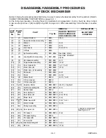
Page 49: ...3 S 5 8 8 Loading Motor Assembly T DM1 DM7 Desolder LDG Belt 2 S 6 9 9 AC Head Assembly T DM1 DM7 S 7 10 2 Tape Guide Assembly T DM1 DM8 P 2 11 10 Door Opener B T DM1 DM8 L 1 L 2 12 11 Pinch Arm B T DM1 DM8 P 3 13 12 Pinch Arm A Assembly T DM1 DM8 14 14 FE Head T DM1 DM9 S 9 15 15 Prism T DM1 DM9 S 10 16 2 Slider Shaft T DM10 S 11 L 3 17 16 C Drive Lever L T DM10 18 16 C Drive Lever R T DM10 19 7 ...

Page 50: ...ing Arm S B Assembly B DM2 DM15 Refer to Alignment Sec Pg 2 4 9 36 35 Loading Arm T B Assembly B DM2 DM15 Refer to Alignment Sec Pg 2 4 9 37 2 25 M Brake T HI Assembly T DM1 DM16 P 6 38 2 25 M Brake S HI Assembly T DM1 DM16 P 7 39 38 Tension Lever Sub Assembly T DM1 DM16 40 39 T Lever Holder T DM1 DM16 L 6 41 2 M Gear HYT T DM1 DM16 C 7 42 2 15 Sensor Gear T DM1 DM16 C 8 43 37 41 Reel T T DM1 DM16...

Page 51: ...2 4 3 U25PALDA 14 13 11 10 12 7 50 8 33 44 42 31 32 41 43 46 45 47 9 37 15 39 40 38 Fig DM1 Top View Fig DM2 Bottom View 35 19 36 24 25 27 26 23 28 34 20 29 22 ...

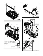
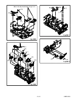
Page 52: ...ushing the locking tab as shown in the right slide and pull up the right side on 2 to release Pin A and Pin B from the slots A Then remove Pin C and Pin D on 2 from the slots B as shown 1 2 A Fig DM4 3 4 5 6 S 3 S 2 S 4 P 1 Fig DM5 7 L 8 A View for A S 5 Fig DM6 Desolder from bottom Lead with Blue Stripe Type B L 9 Type A 50 50 51 ...

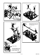
Page 53: ... of 12 are in the grooves of 28 as shown 11 13 12 A 10 L 1 P 3 Adj Screw P 2 L 2 View for A Fig DM8 17 16 18 S 11 L 3 After removing the Screw S 11 while pressing the Locking Tab L 3 remove 16 Fig DM10 8 9 S 7 S 6 LDG Belt A Fig DM7 8 View for A Desolder from bottom Lead with White Stripe 14 15 S 10 S 9 Fig DM9 ...

Page 54: ...2 4 6 U25PALDA S 12 19 Cap Belt Fig DM11 Fig DM12 20 C 1 21 ...

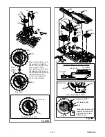
Page 55: ... 31 C 6 Pin of 37 Pin of 34 Position of Mode Lever when installed Pin of 38 23 P 4 C 3 P 4 28 28 23 When installing 23 install the spring P 4 to 28 as shown in the left figure and then install 23 while pressing the spring P 4 to the direction of the arrow in the left figure and confirming that the position of the spring P 4 is placed as shown in the left figure Pin on bottom of 23 Pin on 22 Positi...

Page 56: ...2 4 8 U25PALDA 36 34 33 P 5 L 5 35 Refer to the Alignment Section Page 2 4 9 Fig DM15 L 6 P 7 P 6 C 7 38 44 41 39 43 37 40 turn turn turn 42 C 8 Fig DM16 45 46 47 L 7 Fig DM17 49 48 Slide Fig DM18 ...

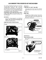
Page 57: ...o the mechanical or electrical parts Alignment points in Eject Position Alignment 1 Loading Arm S and T Assembly Install Loading Arm S and T Assembly so that their triangle marks point to each other as shown in Fig AL2 Alignment 2 Mode Gear Keeping the two triangles pointing at each other install the Loading Arm T Assembly so that the last tooth of the gear meets the most inside teeth of the Mode ...

Page 58: ...ly Install the Rack Assembly so that the first tooth on the gear of the Rack Assembly meets the first groove on the Cam Gear A as shown in Fig AL4 Cam Gear A First tooth First groove on the Cam Gear A Alignment 3 Top View Gear on Rack Assembly Fig AL4 ...

Page 59: ... SECTION VIDEO CASSETTE RECORDER 25A 664 TABLE OF CONTENTS Exploded Views 3 1 1 Mechanical Parts List 3 2 1 Electrical Parts List 3 3 1 Deck Parts List 3 4 1 Sec 3 Exploded views and Parts List Section I Exploded views I Parts List ...

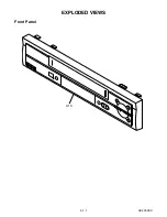
Page 60: ...3 1 1 HC4C0FEX A1X EXPLODED VIEWS Front Panel ...

Page 61: ...21 2L021 2L021 2B5 2L022 2L022 2L022 2L022 2L042 2L031 2L051 2L012 2B18 A4 2L099 2B9 2L041 2L041 AFV CBA A2 2L011 2L011 2L011 2L011 2L011 FUNCTION CBA A7 A3 A10 MAIN CBA 2L041 2B14 JACK CBA 2B7 2B8 2B46 A5 2B49 SENSOR CBA SENSOR CBA VPS CBA A19 ...

Page 62: ...3 1 3 HC4S4PEX Some Ref Numbers are not in sequence X2 X20C X3 X20B X20A X1 X4 S1 Unit S3 S2 S2 A14 Packing ...

Page 63: ...ence Mark Description SLIDUS OIL 150 B2 B35 B553 B410 B411 B494 B567 L1053 B74 B10 L1191 B73 B9 B12 B492 B11 B571 B37 B126 L1466 B501 B8 B121 B426 B560 L1450 L1051 L1467 Floil G 374G Blue grease Chassis Assembly Top View Lubricating Point Chassis Assembly Bottom View Lubricating Point L1468 ...

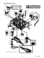
Page 64: ...B565 L1151 B525 B522 B31 L1406 B148 B521 B520 B416 B518 B564 B487 B573 B574 B499 B27 B508 B414 B505 B572 B558 B557 B568 B417 B585 B3 B587 Note Both the TENSION LEVER SUB ASSEMBLY MK11 B27 and the TENSION LEVER ASSEMBLY MK11 B587 can be used B551 Bottom Side Grease point B516 B559 B52 B507 B488 B133 B584 B581 B583 B580 B582 A View for A B578 B579 B579 Deck Mechanism View 2 ...

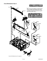
Page 65: ...1 B347 L1321 B359 B529 B360 B361 B359 B529 B360 Type B Type A Note There are two different but interchangeable types of CLEANER LEVER B359 in this model and have different combination with B361 Please see Table 1 for details and combination Refer to DECK PARTS LIST section B361 B359 CLEANER LEVER Type Part No Part No A 0VM411114 Not used 0VM304413 0VM305090 B Table 1 B359 and B361 Combination ...

Page 66: ...cal Parts List 2B9 CUSHION HC460ED 0VM413251 2B14 CUSHION PCB HC460ED 0VM413265 2B18 FIBER TOP CASE HC460ED 0VM412906 2B46 ROHM HOLDER H7770JD See Electrical Parts List 2B49 CHASSIS FIBER HC460ED 0VM413311 2L011 SCREW P TIGHT 3X12 BIND HEAD GBCP3120 2L012 SCREW P TIGHT 3X12 BIND HEAD GBCP3120 2L021 SCREW P TIGHT M3X10 WASHER HEAD GCMP3100 2L022 SCREW P TIGHT M3X10 WASHER HEAD See Electrical Parts ...

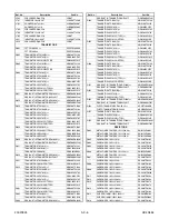
Page 67: ...VSL100 C061 CHIP CERAMIC CAP F Z 0 1µF 50V or CHD1JZB0F104 CHIP CERAMIC CAP F Z 0 1µF 25V or CHD1EZB0F104 CHIP CERAMIC CAP FZ Z 0 1µF 50V or CHD1JZBFZ104 CHIP CERAMIC CAP F Z 0 1µF 50V or CHD1JZ30F104 CHIP CERAMIC CAP F Z 0 1µF 25V or CHD1EZ30F104 CHIP CERAMIC CAP FZ Z 0 1µF 50V CHD1JZ3FZ104 C157 ELECTROLYTIC CAP 1µF 50V M H7 CE1JMAVSL1R0 C158 CHIP CERAMIC CAP B K 1000pF 50V or CHD1JKB0B102 CHIP C...

Page 68: ...RAMIC CAP FZ Z 0 1µF 50V CHD1JZ3FZ104 C329 CHIP CERAMIC CAP CH J 68pF 50V or CHD1JJBCH680 Ref No Description Part No CHIP CERAMIC CAP CG J 68pF 50V or CHD1JJBCG680 CHIP CERAMIC CAP CH J 68pF 50V or CHD1JJ3CH680 CHIP CERAMIC CAP CG J 68pF 50V CHD1JJ3CG680 C330 CERAMIC CAP AX F Z 0 1µF 50V CCA1JZTFZ104 C332 CHIP CERAMIC CAP F Z 0 1µF 50V or CHD1JZB0F104 CHIP CERAMIC CAP F Z 0 1µF 25V or CHD1EZB0F104...

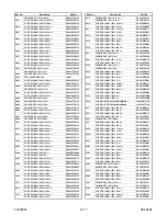
Page 69: ... CAP 22µF 10V M H7 CE1AMAVSL220 C462 CHIP CERAMIC CAP B K 4700pF 50V or CHD1JKB0B472 Ref No Description Part No CHIP CERAMIC CAP B K 4700pF 50V CHD1JK30B472 C463 CHIP CERAMIC CAP B K 0 01µF 50V or CHD1JKB0B103 CHIP CERAMIC CAP B K 0 01µF 50V CHD1JK30B103 C464 CHIP CERAMIC CAP B K 0 01µF 50V or CHD1JKB0B103 CHIP CERAMIC CAP B K 0 01µF 50V CHD1JK30B103 C465 ELECTROLYTIC CAP 10µF 16V M H7 CE1CMAVSL10...

Page 70: ...AMIC CAP CH J 330pF 50V or CHD1JJBCH331 CHIP CERAMIC CAP CG J 330pF 50V or CHD1JJBCG331 Ref No Description Part No CHIP CERAMIC CAP CH J 330pF 50V or CHD1JJ3CH331 CHIP CERAMIC CAP CG J 330pF 50V CHD1JJ3CG331 C526 CHIP CERAMIC CAP B K 4700pF 50V or CHD1JKB0B472 CHIP CERAMIC CAP B K 4700pF 50V CHD1JK30B472 C527 ELECTROLYTIC CAP 22µF 6 3V M H7 CE0KMAVSL220 C529 CHIP CERAMIC CAP B K 0 01µF 50V or CHD1...

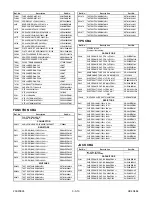
Page 71: ...ODE DZ 11BSAT265 or NDTA00DZ11BS ZENER DIODE MTZJT 7711A or QDTA00MTZJ11 ZENER DIODE MTZJT 7711B QDTB00MTZJ11 D154 ZENER DIODE DZ 11BSAT265 or NDTA00DZ11BS ZENER DIODE MTZJT 7711A or QDTA00MTZJ11 Ref No Description Part No ZENER DIODE MTZJT 7711B QDTB00MTZJ11 D155 ZENER DIODE DZ 11BSAT265 or NDTA00DZ11BS ZENER DIODE MTZJT 7711A or QDTA00MTZJ11 ZENER DIODE MTZJT 7711B QDTB00MTZJ11 D156 ZENER DIODE ...

Page 72: ...r NQSZ0KRA103M Ref No Description Part No RES BUILT IN TRANSISTOR BN1F4M T QQSZ00BN1F4M Q404 TRANSISTOR KTC3199 Y or NQSY0KTC3199 TRANSISTOR KTC3199 GR or NQS10KTC3199 TRANSISTOR 2SC2785 J or QQSJ02SC2785 TRANSISTOR 2SC2785 H or QQSH02SC2785 TRANSISTOR 2SC2785 F or QQSF02SC2785 TRANSISTOR 2SC1815 Y TPE2 or QQSY02SC1815 TRANSISTOR 2SC1815 GR TPE2 QQS102SC1815 Q405 TRANSISTOR KTC3199 Y or NQSY0KTC31...

Page 73: ...RES 1608 1 10W J 18k Ω or RRXAJB5Z0183 CHIP RES 1608 1 10W J 18k Ω RRXAJR5Z0183 Ref No Description Part No R315 CARBON RES 1 6W J 2 4k Ω or RCX6JATZ0242 CARBON RES 1 4W J 2 4k Ω RCX4JATZ0242 R316 CHIP RES 1608 1 10W J 6 8k Ω or RRXAJB5Z0682 CHIP RES 1608 1 10W J 6 8k Ω RRXAJR5Z0682 R317 CHIP RES 1608 1 10W J 1 2k Ω or RRXAJB5Z0122 CHIP RES 1608 1 10W J 1 2k Ω RRXAJR5Z0122 R318 CHIP RES 1608 1 10W ...

Page 74: ... Ω or RRXAJB5Z0393 CHIP RES 1608 1 10W J 39k Ω RRXAJR5Z0393 R467 CHIP RES 1608 1 10W J 6 8k Ω or RRXAJB5Z0682 Ref No Description Part No CHIP RES 1608 1 10W J 6 8k Ω RRXAJR5Z0682 R468 CARBON RES 1 6W J 8 2k Ω or RCX6JATZ0822 CARBON RES 1 4W J 8 2k Ω RCX4JATZ0822 R469 CHIP RES 1608 1 10W J 6 8k Ω or RRXAJB5Z0682 CHIP RES 1608 1 10W J 6 8k Ω RRXAJR5Z0682 R470 CHIP RES 1608 1 10W J 39k Ω or RRXAJB5Z0...

Page 75: ...RXAJB5Z0563 CHIP RES 1608 1 10W J 56k Ω RRXAJR5Z0563 R573 CHIP RES 1608 1 10W J 47k Ω or RRXAJB5Z0473 CHIP RES 1608 1 10W J 47k Ω RRXAJR5Z0473 R611 CHIP RES 1608 1 10W J 10k Ω or RRXAJB5Z0103 CHIP RES 1608 1 10W J 10k Ω RRXAJR5Z0103 Ref No Description Part No R613 CHIP RES 1608 1 10W J 10k Ω or RRXAJB5Z0103 CHIP RES 1608 1 10W J 10k Ω RRXAJR5Z0103 R615 CHIP RES 1608 1 10W J 10k Ω or RRXAJB5Z0103 C...

Page 76: ...T0101HH013 TACT SWITCH SKQSAF001A SST0101AL041 SW671 TACT SWITCH KSM0614B or SST0101HH013 TACT SWITCH SKQSAF001A SST0101AL041 Ref No Description Part No SW673 TACT SWITCH KSM0614B or SST0101HH013 TACT SWITCH SKQSAF001A SST0101AL041 SW675 TACT SWITCH KSM0614B or SST0101HH013 TACT SWITCH SKQSAF001A SST0101AL041 SW676 TACT SWITCH KSM0614B or SST0101HH013 TACT SWITCH SKQSAF001A SST0101AL041 SW677 TACT...

Page 77: ...X1 3 XL03010TE001 L121 BEAD CORE B16 RH 3 5X10X1 3 or XL03010XM001 BEAD CORE HF70BB3 5X10X1 3 XL03010TE001 TRANSISTORS Q101 TRANSISTOR KTA1266 GR or NQS40KTA1266 TRANSISTOR 2SA1015 GR TPE2 QQS102SA1015 Q102 TRANSISTOR KTA1266 GR or NQS40KTA1266 TRANSISTOR 2SA1015 GR TPE2 QQS102SA1015 RESISTORS Ref No Description Part No R101 CARBON RES 1 4W J 1k Ω RCX4JATZ0102 R103 CARBON RES 1 4W J 1k Ω RCX4JATZ0...

Page 78: ...IP CERAMIC CAP F Z 0 1µF 50V or CHD1JZ30F104 CHIP CERAMIC CAP F Z 0 1µF 25V or CHD1EZ30F104 CHIP CERAMIC CAP FZ Z 0 1µF 50V CHD1JZ3FZ104 C20 ELECTROLYTIC CAP 3 3µF 50V M H7 CE1JMASSL3R3 C21 CHIP CERAMIC CAP F Z 0 1µF 50V or CHD1JZ30F104 CHIP CERAMIC CAP F Z 0 1µF 25V or CHD1EZ30F104 CHIP CERAMIC CAP FZ Z 0 1µF 50V CHD1JZ3FZ104 C22 ELECTROLYTIC CAP 10µF 16V M H7 CE1CMASSL100 C24 ELECTROLYTIC CAP 0 ...

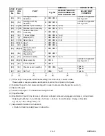
Page 79: ...MBLY 2 MK10 0VSA11531 B148 TG CAP MK6 0VM407664C B300 C DRIVE LEVER R MK11 0VM305068 B303 F DOOR OPENER MK11 0VM203299 B347 GUIDE HOLDER A MK10 0VM304920 B354 SLIDER R MK11 0VM101040 B355 SLIDER L MK11 0VM203296 B359 CLEANER LEVER MK10 or 0VM304413 CLEANER LEVER MK11 0VM305090 B360 CLEANER ROLLER MK9 0VM410032C B361 CL POST MK10 0VM411114 B410 PINCH ARM A ASSEMBLY Y MK11 or 0VSA12807 PINCH ARM A A...

Page 80: ... GEAR HYT N12G5F or 0VM412379 CENTER GEAR MK11 0VM305081 B582 TR GEAR SPRING MK10 0VM411187 B583 REEL WASHER MK9 5 2 1 0 5 0VM410058 B584 TR GEAR SHAFT MK10 0VM411186 B585 PSW 317505 MK11 0VM413663 B587 TENSION LEVER ASSEMBLY MK11 0VSA12075A L1051 SCREW B TIGHT M2 6X6 PAN HEAD GPMB9060 L1053 SCREW S TIGHT M2 6X8 WASHER HEAD GCMS9080 L1151 SCREW SEMS M2 6X4 PAN HEAD CPM39040 L1191 SCREW S TIGHT M2 ...

Page 81: ...25A 664 HC4S4ED ...
Reviews: