


1-3-1
NOTE_1
STANDARD NOTES FOR SERVICING
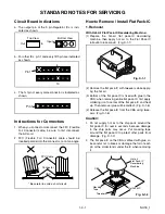
Circuit Board Indications
a. The output pin of the 3 pin Regulator ICs is indi-
cated as shown.
b. For other ICs, pin 1 and every fifth pin are indicated
as shown.
c. The 1st pin of every male connector is indicated as
shown.
Instructions for Connectors
1. When you connect or disconnect the FFC (Flexible
Foil Connector) cable, be sure to first disconnect
the AC cord.
2. FFC (Flexible Foil Connector) cable should be
inserted parallel into the connector, not at an angle.
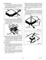
How to Remove / Install Flat Pack-IC
1. Removal
With Hot-Air Flat Pack-IC Desoldering Machine:
.
(1) Prepare the hot-air flat pack-IC desoldering
machine, then apply hot air to the Flat Pack-IC
(about 5 to 6 seconds). (Fig. S-1-1)
(2) Remove the flat pack-IC with tweezers while apply-
ing the hot air.
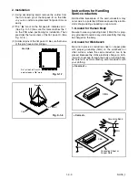
(3) Bottom of the flat pack-IC is fixed with glue to the
CBA; when removing entire flat pack-IC, first apply
soldering iron to center of the flat pack-IC and heat
up. Then remove (glue will be melted). (Fig. S-1-6)
(4) Release the flat pack-IC from the CBA using twee-
zers. (Fig. S-1-6)
Caution:
1. Do not supply hot air to the chip parts around the
flat pack-IC for over 6 seconds because damage
to the chip parts may occur. Put masking tape
around the flat pack-IC to protect other parts from
damage. (Fig. S-1-2)
2. The flat pack-IC on the CBA is affixed with glue, so
be careful not to break or damage the foil of each
pin or the solder lands under the IC when removing
it.
Top View
Out
In
Bottom View
Input
5
10
Pin 1
Pin 1
FFC Cable
Connector
CBA
* Be careful to avoid a short circuit.
Fig. S-1-1
Hot-air
Flat Pack-IC
Desoldering
Machine
CBA
Flat Pack-IC
Tweezers
Masking
Tape
Fig. S-1-2
Summary of Contents for 25A-664
Page 22: ...1 8 3 1 8 4 1 8 5 HC4S4SCM1 Main 1 5 Schematic Diagram ...
Page 23: ...1 8 6 1 8 7 1 8 8 HC4S4SCM2 Main 2 5 Schematic Diagram ...
Page 24: ...1 8 9 1 8 10 1 8 11 HC4S4SCM3 Main 3 5 Schematic Diagram ...
Page 26: ...Main 5 5 Schematic Diagram 1 8 15 1 8 16 HC4S4SCM5 ...
Page 27: ...VPS Schematic Diagram 1 8 17 1 8 18 HC4S4SCV ...
Page 28: ...1 8 19 1 8 20 HC4S4SCF Function Schematic Diagram ...
Page 29: ...AFV Schematic Diagram 1 8 21 1 8 22 HC4S4SCAFV ...
Page 30: ...Jack Schematic Diagram 1 8 23 1 8 24 HC4S4SCJ ...
Page 31: ...1 8 25 1 8 26 Function CBA Top View Function CBA Bottom View BHC400F01018 B ...
Page 33: ...1 8 29 1 8 30 Jack CBA Top View Jack CBA Bottom View BHC400F01018 E ...
Page 54: ...2 4 6 U25PALDA S 12 19 Cap Belt Fig DM11 Fig DM12 20 C 1 21 ...
Page 60: ...3 1 1 HC4C0FEX A1X EXPLODED VIEWS Front Panel ...
Page 81: ...25A 664 HC4S4ED ...


