


- 9 -
4 Specifications
Table 4.1 lists the specifications of the PG interface card.
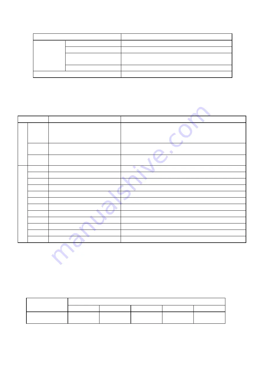
Table 4.1 PG Interface Card Specifications
Item Specifications
Applicable PG
Pulse resolution
20 to 3000 P/R
Maximum response frequency
100 kHz
Pulse output system
Line driver (Equivalent to 26C31 or 26LS31)
Source current: +20 mA (max.), Sink current: -20 mA (max.)
Maximum wiring length
100 m
PG power supply
+5 VDC
±
10%, 300 mA or below
*1
*1
When the PG current consumption exceeds 300 mA, use an external power supply.
5 Terminal
Functions
Table 5.1 lists terminal symbols, names and functions of the option terminals on the PG interface card.
Table 5.1 Option Terminals and Their Specifications
Terminal symbol
Name
Functions
Power
supply
PI
External power supply input
*1
Power input terminal from the external device for the PG
+5 VDC
±
10% input
*2
(A power supply to be connected should assure the PG current consumption or
larger.)
PO
Internal power supply output
*4
Power output terminal for the PG
+5 VDC -0% to +10%, 300 mA output
*3
CM
PG power common
*5
Common terminal for power supply for PG
(Equipotent with [CM] terminal of the inverter)
PG/pulse input
YA
YA(+) phase pulse input from slave PG
Input terminal for A(+) phase signal fed back from the slave PG
*YA
YA(-) phase pulse input from slave PG
Input terminal for A(-) phase signal fed back from the slave PG
YB
YB(+) phase pulse input from slave PG
Input terminal for B(+) phase signal fed back from the slave PG
*YB
YB(-) phase pulse input from slave PG
Input terminal for B(-) phase signal fed back from the slave PG
YZ
YZ(+) phase pulse input from slave PG
Input terminal for Z(+) phase signal fed back from the slave PG
*YZ
YZ(-) phase pulse input from slave PG
Input terminal for Z(-) phase signal fed back from the slave PG
XA
XA(+) phase pulse input from reference PG
Input terminal for A(+) phase signal fed back from the reference PG
*XA
XA(-) phase pulse input from reference PG
Input terminal for A(-) phase signal fed back from the reference PG
XB
XB(+) phase pulse input from reference PG
Input terminal for B(+) phase signal fed back from the reference PG
*XB
XB(-) phase pulse input from reference PG
Input terminal for B(-) phase signal fed back from the reference PG
XZ
XZ(+) phase pulse input from reference PG
Input terminal for Z(+) phase signal fed back from the reference PG
*XZ
XZ(-) phase pulse input from reference PG
Input terminal for Z(-) phase signal fed back from the reference PG
*1
When the PG current consumption exceeds 300 mA, use an external power supply and set a jumper cap at the EXT side on jumper J1. (Refer to
Section 6 "Configuration".)
*2
Use an external power supply whose rating meets the allowable voltage range of the PG. Regulate the external power supply voltage within the PI
voltage range (upper limit +10%), taking into account the voltage drop caused by the PG-inverter wiring impedance. Or, use a wire with a larger
diameter. (Refer to Table5.2)
*3
If the PO voltage level falls below the allowable voltage range of the PG due to voltage drop caused by PG-inverter wiring impedance, use an
external power supply or a wire with a larger diameter.
*4 *5
The PG interface card has two [PO] terminals and three [CM] terminals, each of which is conducting inside the card.
Table 5.2 Recommended Wire Size
PG power supply
requirements
Wiring length (m)
Up to 20
Up to 30
Up to 50
Up to 75
Up to 100
5 V
±
10%
,
300 mA
AWG24
(0.25 mm
2
)
AWG22
(0.34 mm
2
)
AWG20
(0.50 mm
2
)
AWG18
(0.75 mm
2
)
AWG16
(1.25 mm
2
)


