


Fuji Electric Co., Ltd.
3-6
MT6M12343 Rev.1.0
Dec.-2016
Chapter 3
Detail of Signal Input/Output Terminals
2. Power Supply Terminals of High Side VB(U,V,W)
The VB(*) voltage, which is the voltage difference between VB(U,V,W) and U,V,W, provides the supply
to the HVICs within the IPM. This supply must be in the range of 13.0~18.5V to ensure that the HVICs
can fully drive the upper side IGBTs. The IPM includes UV function for the VB(*) to ensure that the
HVICs do not drive the upper side IGBTs, if the VB(*) voltage drops below a specified voltage (refer to
the datasheet). This function prevents the IGBT from operating in a high dissipation mode. Please note
here, that the UV (under voltage protection) function of any high side section acts only on the triggered
channel without any feedback to the control level.
In case of using bootstrap circuit, the IGBT drive power supply for upper side arms can be composed
of one common power supply with a lower side arm. In the conventional IPM, three independent
insulated power supplies were necessary for IGBT drive circuit of upper side arm.
The power supply of the upper side arm is charged when the lower side IGBT is turned on or when
freewheel current flows the lower side FWD. Table 3-2 describes the behavior of the IPM for various
control supply voltages. The control supply should be well filtered with a low impedance capacitor and a
high frequency decoupling capacitor connected close to the terminals in order to prevent malfunction of
the internal control IC caused by a high frequency noise on the power supply.
When control supply voltage (VB(U)-U,VB(V)-V and VB(W)-W) falls down under UV (Under Voltage
protection) level, only triggered phase IGBT is off-state regardless the input signal condition.
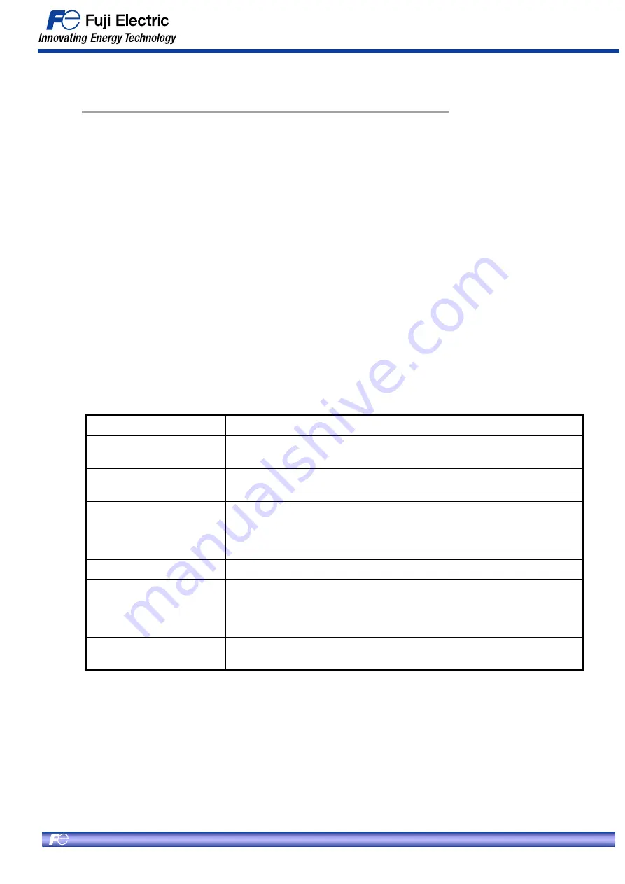
Control Voltage Range [V]
IPM operations
0 ~ 4
HVICs are not activated. UV does not operate. dV/dt noise on the main P-
N supply might trigger the IGBTs.
4 ~ 12.5
HVICs start to operate. As the UV is activated, control input signals are
blocked.
12.5 ~ 13
UV is reset. The upper side IGBTs are operated in accordance with the
control gate input. Driving voltage is below the recommended range, so
V
CE(sat)
and the switching loss will be larger than that under normal
condition.
13 ~ 18.5
Normal operation. This is the recommended operating condition.
18.5 ~ 20
The upper side IGBTs are still operating. Because driving voltage is
above the recommended rage, IGBT’s switching is faster. It causes
increasing system noise. And peak short circuit current might be too large
for proper operation of the short circuit protection.
Over 20
Control circuit in the IPM might be damaged. It is recommended to insert
a Zener diode between each pair of high side power supply terminals.
Table 3-2 Functions versus high side bias voltage for IGBT driving VB(*)
1. Voltage range of high side bias voltage for IGBT driving terminals VB(U,V,W)


