background image


Advance Information

MC68HC(7)08KH12

 — 

Rev. 1.1

102

Freescale Semiconductor

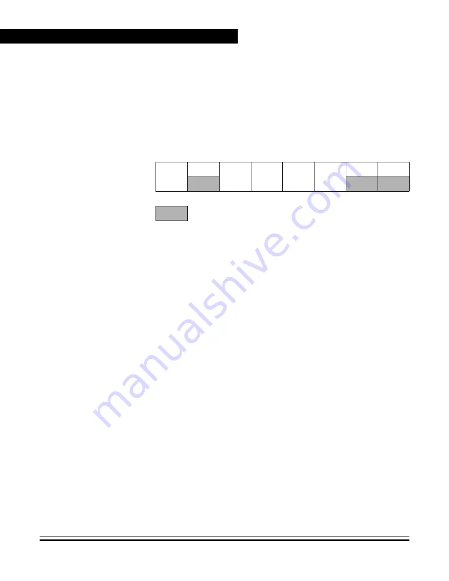
8.6.1 PLL Control Register (PCTL)

The PLL control register contains the interrupt enable and flag bits, the 
on/off switch, the base clock selector bit, the prescaler bits, and the VCO 
power of two range selector bits.

PLLIE — PLL Interrupt Enable Bit 

This read/write bit enables the PLL to generate an interrupt request 
when the LOCK bit toggles, setting the PLL flag, PLLF. When the 
AUTO bit in the PLL bandwidth control register (PBWC) is clear, 
PLLIE cannot be written and reads as logic zero. Reset clears the 
PLLIE bit.

1 = PLL interrupts enabled
0 = PLL interrupts disabled

PLLF — PLL Interrupt Flag Bit

This read-only bit is set whenever the LOCK bit toggles. PLLF 
generates an interrupt request if the PLLIE bit also is set. PLLF 
always reads as logic zero when the AUTO bit in the PLL bandwidth 
control register (PBWC) is clear. Clear the PLLF bit by reading the 
PLL control register. Reset clears the PLLF bit.

1 = Change in lock condition
0 = No change in lock condition

NOTE:

Do not inadvertently clear the PLLF bit. Any read or read-modify-write 
operation on the PLL control register clears the PLLF bit. 

Address:

$003A

Bit  7

6

5

4

3

2

1

Bit  0

Read:

PLLIE

PLLF

PLLON

BCS

PRE1

PRE2

0

0

Write:

Reset:

0

0

1

0

1

0

0

0

= Unimplemented

Figure 8-3. PLL Control Register (PCTL)

Summary of Contents for MC68HC08KH12

Page 1: ...M68HC08 Microcontrollers freescale com MC68HC08KH12 Data Sheet Rev 1 1 MC68HC08KH12 H July 15 2005...

Page 2: ......

Page 3: ...al Processor Unit CPU 51 Section 7 System Integration Module SIM 61 Section 8 Clock Generator Module CGM 87 Section 9 Universal Serial Bus Module USB 113 Section 10 Monitor ROM MON 149 Section 11 Time...

Page 4: ...Advance Information MC68HC 7 08KH12 Rev 1 1 4 Freescale Semiconductor...

Page 5: ...llator Pins OSC1 and OSC2 30 1 5 4 External Reset Pin RST 30 1 5 5 External Interrupt Pin IRQ1 VPP 30 1 5 6 USB Data Pins DPLUS0 DPLUS4 and DMINUS0 DMINUS4 30 1 5 7 Voltage Regulator Out REGOUT 30 1 5...

Page 6: ...ents 47 4 2 Introduction 47 4 3 Functional Description 47 Section 5 Configuration Register CONFIG 5 1 Contents 49 5 2 Introduction 49 5 3 Functional Description 49 Section 6 Central Processor Unit CPU...

Page 7: ...code Reset 70 7 4 2 4 Illegal Address Reset 70 7 4 2 5 Universal Serial Bus Reset 70 7 5 SIM Counter 71 7 5 1 SIM Counter During Power On Reset 71 7 5 2 SIM Counter During Stop Mode Recovery 71 7 5 3...

Page 8: ...8 Base Clock Selector Circuit 96 8 4 9 CGM External Connections 96 8 5 I O Signals 98 8 5 1 Crystal Amplifier Input Pin OSC1 98 8 5 2 Crystal Amplifier Output Pin OSC2 98 8 5 3 External Filter Capacit...

Page 9: ...rt Control Register HDP1CR HDP4CR 121 9 4 3 USB SIE Timing Interrupt Register SIETIR 123 9 4 4 USB SIE Timing Status Register SIETSR 125 9 4 5 USB HUB Address Register HADDR 127 9 4 6 USB HUB Interrup...

Page 10: ...g Monitor Mode 152 10 4 2 Data Format 154 10 4 3 Echoing 154 10 4 4 Break Signal 155 10 4 5 Commands 155 10 4 6 Baud Rate 159 Section 11 Timer Interface Module TIM 11 1 Contents 161 11 2 Introduction...

Page 11: ...SC1 177 11 9 5 TIM Channel Registers TCH0H L TCH1H L 181 Section 12 I O Ports 12 1 Contents 183 12 2 Introduction 184 12 3 Port A 186 12 3 1 Port A Data Register PTA 186 12 3 2 Data Direction Register...

Page 12: ...ion 208 13 4 I O Signals 209 13 4 1 CGMXCLK 209 13 4 2 COPCTL Write 209 13 4 3 Power On Reset 210 13 4 4 Internal Reset 210 13 4 5 Reset Vector Fetch 210 13 4 6 COPD COP Disable 210 13 4 7 COPRS COP R...

Page 13: ...t Enable Register 226 15 5 Port E Keyboard Interrupt Block Diagram 228 15 5 1 Port E Keyboard Interrupt Functional Description 229 15 5 2 Port E Keyboard Initialization 230 15 5 3 Port E Keyboard Inte...

Page 14: ...tatus and Control Register BRKSCR 245 16 5 2 Break Address Registers BRKH and BRKL 245 16 6 Low Power Modes 246 16 6 1 Wait Mode 246 16 6 2 Stop Mode 246 Section 17 Preliminary Electrical Specificatio...

Page 15: ...256 17 14 TImer Interface Module Characteristics 256 17 15 Clock Generation Module Characteristics 257 17 15 1 CGM Component Specifications 257 17 15 2 CGM Electrical Specifications 257 17 15 3 Acquis...

Page 16: ...Advance Information MC68HC 7 08KH12 Rev 1 1 16 Freescale Semiconductor...

Page 17: ...cumulator A 53 6 3 Index Register H X 54 6 4 Stack Pointer SP 55 6 5 Program Counter PC 56 6 6 Condition Code Register CCR 57 7 1 SIM Block Diagram 63 7 2 SIM I O Register Summary 64 7 3 SIM Clock Sig...

Page 18: ...Port Control Register HRPCR 120 9 3 USB HUB Downstream Port Control Registers HDP1CR HDP4CR 121 9 4 USB SIE Timing Interrupt Register SIETIR 123 9 5 USB SIE Timing Status Register SIETSR 125 9 6 USB H...

Page 19: ...1 7 CHxMAX Latency 181 11 8 TIM Channel Registers TCH0H L TCH1H L 182 12 1 Port A Data Register PTA 186 12 2 Data Direction Register A DDRA 187 12 3 Port A I O Circuit 187 12 4 Port B Data Register PT...

Page 20: ...Status and Control Register KBDSCR 225 15 3 Port D Keyboard Interrupt Enable Register KBDIER 226 15 4 Port E Keyboard Interrupt Block Diagram 228 15 5 Port E Keyboard Status and Control Register KBESC...

Page 21: ...ol Register Summary 117 9 2 HUB Data Register Summary 119 9 3 Embedded Device Control Register Summary 135 9 4 Embedded Device Data Register Summary 136 10 1 Mode Selection 152 10 2 Mode Differences 1...

Page 22: ...2 Port A Pin Functions 188 12 3 Port B Pin Functions 190 12 4 Port C Pin Functions 192 12 5 Port D Pin Functions 195 12 6 Port E Pin Functions 198 12 7 Port F Pin Functions 204 13 1 COP I O Port Regi...

Page 23: ...2 and VSS2 29 1 5 3 Oscillator Pins OSC1 and OSC2 30 1 5 4 External Reset Pin RST 30 1 5 5 External Interrupt Pin IRQ1 VPP 30 1 5 6 USB Data Pins DPLUS0 DPLUS4 and DMINUS0 DMINUS4 30 1 5 7 Voltage Reg...

Page 24: ...ce M68HC08 Architecture Fully Upward Compatible Object Code with M6805 M146805 and M68HC05 Families 6 MHz Internal Bus Operation Low Power Design Fully Static with Stop and Wait Modes 12 KBytes of Use...

Page 25: ...e transmit buffer and 8 byte receive buffer Device Interrupt Endpoints Endpoint1 and Endpoint2 share with 8 byte transmit buffer On chip 3 3V regulator for USB Transceiver System Protection Features O...

Page 26: ...unctions 16 Addressing Modes Eight More Than the HC05 16 Bit Index Register and Stack Pointer Memory to Memory Data Transfers Fast 8 8 Multiply Instruction Fast 16 8 Divide Instruction Binary Coded De...

Page 27: ...0 KBE0 VDD2 VSS2 VSSA VDDA CGMXFC DPLUS4 TCH0 PTE1 TCH1 PTE2 TCLK PTE0 PORT C DDRC PORT B DDRB PORT A DDRA PORT D DDRD PORT E DDRE PORT F DDRF Embedded USB Function 384 bytes RAM 12k bytes ROM OTPROM...

Page 28: ...LUS4 DMINUS4 14 15 16 PTB4 PTB5 PTB6 PTB7 PTA0 PTA1 PTA2 PTA3 PTB3 PTB2 PTB1 PTB0 PTD7 KBD7 47 46 45 44 42 42 41 40 39 38 37 36 PTD6 KBD6 PTD5 KBD5 PTD4 KBD4 35 34 33 PTF5 KBF5 PTF4 KBF4 PTF3 KBF3 PTF...

Page 29: ...supply Fast signal transitions on MCU pins place high short duration current demands on the power supply To prevent noise problems take special care to provide power supply bypassing at the MCU as Fi...

Page 30: ...nterrupt pin IRQ1 VPP is also the OTPROM programming power pin The IRQ1 VPP pin contain an internal pullup device See Section 14 External Interrupt IRQ 1 5 6 USB Data Pins DPLUS0 DPLUS4 and DMINUS0 DM...

Page 31: ...e configurable to be LED Direct Drive ports Each pin contains a software configurable pull up device when the pin is configured as an input See 12 9 Port Options 1 5 11 Port D I O Pins PTD7 KBD7 PTD0...

Page 32: ...or 1 5 13 Port F I O Pins PTF7 KBF7 PTF0 KBF0 PTF7 KBF7 PTF0 KBF0 are general purpose bidirectional I O port pins See Section 12 I O Ports Any or all of the port F pins can be programmed to serve as e...

Page 33: ...Section 2 Memory Map 2 1 Contents 2 2 Introduction 33 2 3 I O Section 35 2 4 Monitor ROM 43 2 2 Introduction The CPU08 can address 64 Kbytes of memory space The memory map shown in Figure 2 1 include...

Page 34: ...3 BREAK FLAG CONTROL REGISTER BFCR FE04 INTERRUPT STATUS REGISTER 1 INT1 FE05 INTERRUPT STATUS REGISTER 2 INT2 FE06 RESERVED FE07 RESERVED FE08 FE0B RESERVED 4 BYTES FE0C BREAK ADDRESS HIGH REGISTER B...

Page 35: ...ddresses FE00 Break Status Register BSR FE01 Reset Status Register RSR FE02 Reserved FE03 Break Flag Control Register BFCR FE04 Interrupt Status Register 1 INT1 FE05 Interrupt Status Register 2 INT2 F...

Page 36: ...ection Register D DDRD R DDRD7 DDRD6 DDRD5 DDRD4 DDRD3 DDRD2 DDRD1 DDRD0 W 0008 Port E Data Register PTE R 0 0 0 PTE4 PTE3 PTE2 PTE1 PTE0 W 0009 Port F Data Register PTF R PTF7 PTF6 PTF5 PTF4 PTF3 PTF...

Page 37: ...H0H R Bit 15 14 13 12 11 10 9 Bit 8 W 0018 TIM Channel 0 Register Low TCH0L R Bit 7 6 5 4 3 2 1 Bit 0 W 0019 TIM Channel 1 Status and Control Register TSC1 R CH1F CH1IE 0 MS1A ELS1B ELS1A TOV1 CH1MAX...

Page 38: ...E0D6 R DE0R67 DE0R66 DE0R65 DE0R64 DE0R63 DE0R62 DE0R61 DE0R60 W DE0T67 DE0T66 DE0T65 DE0T64 DE0T63 DE0T62 DE0T61 DE0T60 0027 USB Embedded Device Endpoint 0 Data Register 7 DE0D7 R DE0R77 DE0R76 DE0R7...

Page 39: ...E0T42 HE0T41 HE0T40 0035 USB HUB Endpoint 0 Data Register 5 HE0D5 R HE0R57 HE0R56 HE0R55 HE0R54 HE0R53 HE0R52 HE0R51 HE0R50 W HE0T57 HE0T56 HE0T55 HE0T54 HE0T53 HE0T52 HE0T51 HE0T50 0036 USB HUB Endpo...

Page 40: ...Embedded Device Address Register DADDR R DEVEN DADD6 DADD5 DADD4 DADD3 DADD2 DADD1 DADD0 W 0049 USB Embedded Device Interrupt Register 0 DIR0 R TXD0F RXD0F 0 0 TXD0IE RXD0IE 0 0 W TXD0FR RXD0FR 004A...

Page 41: ...E W 0057 USB SIE Timing Status Register SIETSR R RSTF 0 LOCKF 0 0 0 0 0 W RSTFR LOCKFR SOFFR EOF2FR EOPFR TRANFR 0058 USB HUB Address Register HADDR R USBEN ADD6 ADD5 ADD4 ADD3 ADD2 ADD1 ADD0 W 0059 U...

Page 42: ...1 IF10 IF9 IF8 IF7 W R R R R R R R R FE06 Reserved R W FE07 Reserved R W FE08 Unimplemented R W FE09 Unimplemented R W FE0A Unimplemented R W FE0B Unimplemented R W FE0C Break Address Register High BR...

Page 43: ...yboard Vector Low FFEC Port E Keyboard Vector High FFED Port E Keyboard Vector Low FFEE TIM Overflow Vector High FFEF TIM Overflow Vector Low FFF0 TIM Channel 1 Vector High FFF1 TIM Channel 1 Vector L...

Page 44: ...Advance Information MC68HC 7 08KH12 Rev 1 1 44 Freescale Semiconductor...

Page 45: ...space NOTE For correct operation the stack pointer must point only to RAM locations Within page zero are 160 bytes of RAM Because the location of the stack RAM is programmable all page zero RAM locat...

Page 46: ...e call the CPU uses two bytes of the stack to store the return address The stack pointer decrements during pushes and increments during pulls NOTE Be careful when using nested subroutines The CPU may...

Page 47: ...08KH12 OTP part the ROM is replaced with 11 776 bytes One Time Programmable OTP ROM Programming tools are available from Freescale Contact your local Freescale representative for more information 4 3...

Page 48: ...Advance Information MC68HC 7 08KH12 Rev 1 1 48 Freescale Semiconductor...

Page 49: ...er operating properly module COP COP reset period COPRS 213 24 CGMXCLK or 218 24 CGMXCLK 5 3 Functional Description The configuration register is used in the initialization of various options The conf...

Page 50: ...MXCLK cycles NOTE Exiting stop mode by pulling reset will result in the long stop recovery If using an external crystal do not set the SSREC bit COPRS COP reset period selection bit 1 COP reset cycle...

Page 51: ...x Register H X 54 6 4 3 Stack Pointer SP 55 6 4 4 Program Counter PC 56 6 4 5 Condition Code Register CCR 57 6 5 Arithmetic Logic Unit ALU 59 6 2 Introduction This section describes the central proces...

Page 52: ...8 MHz CPU Internal Bus Frequency 64 Kbyte Program Data Memory Space 16 Addressing Modes Memory to Memory Data Moves Without Using Accumulator Fast 8 Bit by 8 Bit Multiply and 16 Bit by 8 Bit Divide I...

Page 53: ...r to hold operands and the results of arithmetic logic operations ACCUMULATOR A INDEX REGISTER H X STACK POINTER SP PROGRAM COUNTER PC CONDITION CODE REGISTER CCR CARRY BORROW FLAG ZERO FLAG NEGATIVE...

Page 54: ...r and X is the lower byte H X is the concatenated 16 bit index register In the indexed addressing modes the CPU uses the contents of the index register to determine the conditional address of the oper...

Page 55: ...ments as data is pulled from the stack In the stack pointer 8 bit offset and 16 bit offset addressing modes the stack pointer can function as an index register to access data on the stack The CPU uses...

Page 56: ...very time an instruction or operand is fetched Jump branch and interrupt operations load the program counter with an address other than that of the next sequential location During reset the program co...

Page 57: ...ement overflow occurs The signed branch instructions BGT BGE BLE and BLT use the overflow flag 1 Overflow 0 No overflow H Half Carry Flag The CPU sets the half carry flag when a carry occurs between a...

Page 58: ...hen the user must stack and unstack H using the PSHH and PULH instructions After the I bit is cleared the highest priority interrupt request is serviced first A return from interrupt RTI instruction p...

Page 59: ...a borrow Some instructions such as bit test and branch shift and rotate also clear or set the carry borrow flag 1 Carry out of bit 7 0 No carry out of bit 7 6 5 Arithmetic Logic Unit ALU The ALU perf...

Page 60: ...Advance Information MC68HC 7 08KH12 Rev 1 1 60 Freescale Semiconductor...

Page 61: ...eset 68 7 4 2 2 Computer Operating Properly COP Reset 69 7 4 2 3 Illegal Opcode Reset 70 7 4 2 4 Illegal Address Reset 70 7 4 2 5 Universal Serial Bus Reset 70 7 5 SIM Counter 71 7 5 1 SIM Counter Dur...

Page 62: ...th the CPU the SIM controls all MCU activities A block diagram of the SIM is shown in Figure 7 1 Figure 7 2 is a summary of the SIM I O registers The SIM is a system state controller that coordinates...

Page 63: ...TER INTERRUPT CONTROL AND PRIORITY DECODE MODULE STOP MODULE WAIT CPU STOP FROM CPU CPU WAIT FROM CPU SIMOSCEN TO CGM CGMOUT FROM CGM INTERNAL CLOCKS MASTER RESET CONTROL RESET PIN LOGIC ILLEGAL OPCOD...

Page 64: ...Break Flag Control Register BFCR Read BCFE R R R R R R R Write Reset 0 FE04 Interrupt Status Register 1 INT1 Read IF6 IF5 IF4 IF3 IF2 IF1 0 0 Write R R R R R R R R Reset 0 0 0 0 0 0 0 0 FE05 Interrupt...

Page 65: ...In user mode the internal bus frequency is the oscillator frequency CGMXCLK divided by four Table 7 1 Signal Name Conventions Signal Name Description CGMXCLK Buffered OSC1 from the oscillator CGMOUT T...

Page 66: ...the stop delay timeout This timeout is selectable as 4096 or 32 CGMXCLK cycles See 7 7 2 Stop Mode In wait mode the CPU clocks are inactive The SIM also produces two sets of clocks for other modules R...

Page 67: ...ws the relative timing Figure 7 4 External Reset Timing 7 4 2 Active Resets from Internal Sources All internal reset sources actively pull the RST pin low for 32 CGMXCLK cycles to allow resetting of e...

Page 68: ...nts out 4096 CGMXCLK cycles Sixty four CGMXCLK cycles later the CPU and memories are released from reset to allow the reset vector sequence to occur At power on the following events occur A POR pulse...

Page 69: ...h 5 of the SIM counter The SIM counter output which occurs at least every 212 24 CGMXCLK cycles drives the COP counter The COP should be serviced as soon as possible out of reset to guarantee the maxi...

Page 70: ...all internal reset sources 7 4 2 5 Universal Serial Bus Reset The USB module will detect a reset signal on the bus by the presence of an extended SE0 at the USB data pins of the upstream port The res...

Page 71: ...ator to drive the bus clock state machine 7 5 2 SIM Counter During Stop Mode Recovery The SIM counter also is used for stop mode recovery The STOP instruction clears the SIM counter After an interrupt...

Page 72: ...errupt temporarily changes the sequence of program execution to respond to a particular event Figure 7 8 flow charts the handling of system interrupts Interrupts are latched and arbitration is perform...

Page 73: ...g NO NO NO YES NO NO YES NO YES YES FROM RESET BREAK I BIT SET IRQ1 INTERRUPT USB INTERRUPT FETCH NEXT INSTRUCTION UNSTACK CPU REGISTERS STACK CPU REGISTERS SET I BIT LOAD PC WITH INTERRUPT VECTOR EXE...

Page 74: ...Figure 7 10 Interrupt Recovery 7 6 1 1 Hardware Interrupts A hardware interrupt does not stop the current instruction Processing of a hardware interrupt begins after completion of the current instruc...

Page 75: ...pt is serviced before the LDA instruction is executed Figure 7 11 Interrupt Recognition Example The LDA opcode is prefetched by both the INT1 and INT2 RTI instructions However in the case of the INT1...

Page 76: ...seful for debugging Table 7 3 Interrupt Sources Source Flag Mask 1 INT Register Flag Priority 2 Vector Address SWI Instruction 0 FFFC FFFD IRQ1 Pin IRQF1 IMASK1 IF1 1 FFFA FFFB HUB Start of Frame Inte...

Page 77: ...t KEYDF IMASKD IF9 9 FFEA FFEB Port F Keyboard Pin Interrupt KEYFF IMASKF IF10 10 FFE8 FFE9 Phase locked Loop Interrupt PLLF PLLIE IF11 11 FFE6 FFE7 1 The I bit in the condition code register is a glo...

Page 78: ...upt request present 0 No interrupt request present 7 6 2 3 Interrupt Status Register 3 Bits 7 0 Always read 0 Address FE05 Bit 7 6 5 4 3 2 1 Bit 0 Read 0 0 0 IF11 IF10 IF9 IF8 IF7 Write R R R R R R R...

Page 79: ...rly initializing the break clear flag enable bit BCFE in the break flag control register BFCR Protecting flags in break mode ensures that set flags will not be cleared while in break mode This protect...

Page 80: ...clocks are inactive Refer to the wait mode subsection of each module to see if the module is active or inactive in wait mode Some modules can be programmed to be active in wait mode Wait mode can als...

Page 81: ...ator signals CGMOUT and CGMXCLK in stop mode stopping the CPU and peripherals Stop recovery time is selectable using the SSREC bit in the configuration register CONFIG If SSREC is set stop recovery is...

Page 82: ...the recovery period Figure 7 18 shows stop mode entry timing NOTE To minimize stop current all pins configured as inputs should be driven to a logic 1 or logic 0 Figure 7 18 Stop Mode Entry Timing Fig...

Page 83: ...errupt Clear SBSW by writing a logic zero to it Reset clears SBSW 1 Stop mode or wait mode was exited by break interrupt 0 Stop mode or wait mode was not exited by break interrupt SBSW can be read wit...

Page 84: ...reak service routine software This code should be executed at the end of the break service routine software HIBYTE EQU 5 LOBYTE EQU 6 If not SBSW do RTI BRCLR SBSW BSR RETURN See if wait mode or stop...

Page 85: ...sed by an illegal opcode 0 POR or read of RSR ILAD Illegal Address Reset Bit opcode fetches only 1 Last reset caused by an opcode fetch from an illegal address 0 POR or read of RSR USB Universal Seria...

Page 86: ...r Flag Enable Bit This read write bit enables software to clear status bits by accessing status registers while the MCU is in a break state To clear status bits during the break state the BCFE bit mus...

Page 87: ...8 4 8 Base Clock Selector Circuit 96 8 4 9 CGM External Connections 96 8 5 I O Signals 98 8 5 1 Crystal Amplifier Input Pin OSC1 98 8 5 2 Crystal Amplifier Output Pin OSC2 98 8 5 3 External Filter Ca...

Page 88: ...generator module CGM The CGM generates the crystal clock signal CGMXCLK which operates at the frequency of the crystal The CGM also generates the base clock signal CGMOUT which is based on either the...

Page 89: ...l Mode for Low Jitter Operation Automatic Frequency Lock Detector CPU Interrupt on Entry or Exit from Locked Condition 8 4 Functional Description The CGM consists of three major submodules Crystal osc...

Page 90: ...LLED OSCILLATOR AUTOMATIC MODE CONTROL LOCK DETECTOR CLOCK CGMXCLK CGMOUT CGMVDV CGMVCLK SIMOSCEN INTERRUPT CONTROL CGMINT CGMRDV PLL ANALOG 2 CGMRCLK OSC2 OSC1 SELECT CIRCUIT VDDA CGMXFC VSSA LOCK AU...

Page 91: ...re precise timing for operation The duty cycle of CGMXCLK is not guaranteed to be 50 and depends on external factors including the crystal and related external components An externally generated clock...

Page 92: ...aler divides the VCO clock by a power of two factor P and the modulo divider reduces the VCO clock by a factor N The dividers output is the VCO feedback clock CGMVDV running at a frequency fVDV fVCLK...

Page 93: ...e 8 4 8 Base Clock Selector Circuit The PLL is automatically in tracking mode when not in acquisition mode or when the ACQ bit is set 8 4 5 Manual and Automatic PLL Bandwidth Modes This CGM is optimiz...

Page 94: ...fications for more information The LOCK bit is a read only indicator of the locked state of the PLL The LOCK bit is set when the VCO frequency is within a certain tolerance LOCK and is cleared when th...

Page 95: ...he PLL registers accordingly a In the PRE bits of the PLL control register PCTL program the binary equivalent of P b In the PLL multiplier select register low PMSL and the PLL multiplier select regist...

Page 96: ...lock frequency is one fourth the frequency of the selected clock CGMXCLK or CGMPCLK The BCS bit in the PLL control register PCTL selects which clock drives CGMOUT The VCO clock cannot be selected as t...

Page 97: ...uency crystals Refer to the crystal manufacturer s data for more information Figure 8 2 also shows the external components for the PLL Bypass capacitor CBYP Filter capacitor CF Routing should be done...

Page 98: ...NOTE To prevent noise problems CF should be placed as close to the CGMXFC pin as possible with minimum routing distances and no routing of other signals across the CF connection 8 5 4 PLL Analog Power...

Page 99: ...cillator circuit Figure 8 2 shows only the logical relation of CGMXCLK to OSC1 and OSC2 and may not represent the actual circuitry The duty cycle of CGMXCLK is unknown and may depend on the crystal an...

Page 100: ...ister PCTL See 8 6 1 PLL Control Register PCTL PLL bandwidth control register PBWC See 8 6 2 PLL Bandwidth Control Register PBWC PLL multiplier select registers PMSH PMSL See 8 6 3 PLL Multiplier Sele...

Page 101: ...UL9 MUL8 Write Reset 0 0 0 0 0 0 0 0 003D PLL Multiplier Select Register Low PMSL Read MUL7 MUL6 MUL5 MUL4 MUL3 MUL2 MUL1 MUL0 Write Reset 0 0 0 0 0 0 1 0 003E Unimplemented Read Write Reset 003F PLL...

Page 102: ...eset clears the PLLIE bit 1 PLL interrupts enabled 0 PLL interrupts disabled PLLF PLL Interrupt Flag Bit This read only bit is set whenever the LOCK bit toggles PLLF generates an interrupt request if...

Page 103: ...ld in stasis See 8 4 8 Base Clock Selector Circuit Reset clears the BCS bit 1 Selects the VCO clocks for the base clock CGMPCLK divided by two drives CGMOUT CGMVCLK 48MHz drives USBCLK 0 Selects the c...

Page 104: ...y output of 48MHz for the USB module automatic control should be set Reset clears the AUTO bit 1 Automatic bandwidth control recommended 0 Manual bandwidth control LOCK Lock Indicator Bit When the AUT...

Page 105: ...er the PLL is in acquisition or tracking mode In automatic bandwidth control mode AUTO 1 the last written value from manual operation is stored in a temporary location and is recovered when manual ope...

Page 106: ...e PLL reference divider select register contains the programming information for the modulo reference divider RDS 3 0 Reference Divider Select Bits These read write bits control the modulo reference d...

Page 107: ...rupt and appropriate precautions should be taken If the application is not frequency sensitive interrupts should be disabled to prevent PLL interrupt service routines from impeding software performanc...

Page 108: ...tions the most critical PLL design parameters Proper design and use of the PLL ensures the highest stability and lowest acquisition lock times 8 9 1 Acquisition Lock Time Definitions Typical control s...

Page 109: ...nce TRK Acquisition time is based on an initial frequency error fDES fORIG fDES of not more than 100 percent In automatic bandwidth control mode See 8 4 5 Manual and Automatic PLL Bandwidth Modes acqu...

Page 110: ...itor size The size of the capacitor also is related to the stability of the PLL If the capacitor is too small the PLL cannot make small enough adjustments to the voltage and the system cannot lock If...

Page 111: ...size so round to the nearest available size If the value is between two different sizes choose the higher value for better stability Choosing the lower size may seem attractive for acquisition time i...

Page 112: ...entry tolerance TRK before exiting acquisition mode A certain number of clock cycles nTRK is required to ascertain that the PLL is within the lock mode entry tolerance LOCK Therefore the acquisition t...

Page 113: ...Control Register 0 HCR0 129 9 4 8 USB HUB Endpoint1 Control Data Register HCDR 131 9 4 9 USB HUB Status Register HSR 132 9 4 10 USB HUB Endpoint 0 Data Registers 0 7 HE0D0 HE0D7 134 9 5 I O Register...

Page 114: ...SB reset support Suspend and resume operations Remote Wakeup support STALL NAK and ACK handshake generation Features of the HUB function include the following HUB Control Endpoint 0 8 byte transmit bu...

Page 115: ...t device connect disconnect detection bus fault detection and recovery and full low speed device traffic control Endpoint 0 of the hub sub module functions as a receive transmit control endpoint Endpo...

Page 116: ...he buffering of data between the USB hub function and the CPU These registers are shown in Table 9 1 and Table 9 2 D0 D0 TRANSCEIVER 3 3V OUT CPU BUS TRANSCEIVER D1 D4 D1 D4 ROOR PORT DOWNSTREAM PORTS...

Page 117: ...USP3 0 D3 D3 Write Reset 0 0 0 0 0 0 X X 0054 USB HUB Downstream Port 4 Control Register HDP4CR Read PEN4 LOWSP4 RST4 RESUM4 SUSP4 0 D4 D4 Write Reset 0 0 0 0 0 0 X X 0055 Unimplemented Read Write Res...

Page 118: ...0 0 0 005C USB HUB Endpoint 1 Control and Data Register HCDR Read STALL1 PNEW PCHG5 PCHG4 PCHG3 PCHG2 PCHG1 PCHG0 Write Reset 0 0 0 0 0 0 0 0 005D USB HUB Status Register HSR Read RSEQ SETUP TX1ST 0...

Page 119: ...dpoint 0 Data Register 3 HE0D3 Read HE0R37 HE0R36 HE0R35 HE0R34 HE0R33 HE0R32 HE0R31 HE0R30 Write HE0T37 HE0T36 HE0T35 HE0T34 HE0T33 HE0T32 HE0T31 HE0T30 Reset X X X X X X X X 0034 USB HUB Endpoint 0...

Page 120: ...t also determines the latch scheme for the data lines of the root port and the downstream port When this bit is 1 the current state shown on the data lines will be reflected to the data register D D d...

Page 121: ...P4CR PEN1 PEN4 Downstream Port Enable Control Bit This read write bit determines whether the enabled or disabled state should be assigned to the downstream port Setting this bit 1 to enable the port a...

Page 122: ...write bit forces a reset signal SE0 state onto the USB downstream port data lines This bit can be set by the host request SetPortFeature PORT_RESET only Software should control the timing of the forc...

Page 123: ...cking occurs at the next EOF2 point when this bit is set Reset clears this bit 1 Force downstream port enters the selective suspend mode 0 Default D1 D1 to D4 D4 Downstream Port Differential Data Thes...

Page 124: ...ster Reset clears this bit Writing to EOF2F has no effect 1 Frame timer counts to the EOF2 point 0 Frame timer does not count to the EOF2 point EOPF End of Packet Detect Flag This read only bit is set...

Page 125: ...OPIE End of Packet Detect Interrupt Enable This read write bit enables the USB to generate a interrupt request when the EOPF bit becomes set Reset clears the bit 1 USB interrupt enabled for End of Pac...

Page 126: ...to the LOCKFR bit Reset clears this bit LOCKFR Clear Frame Timer Locked Flag Writing a logic 1 to this write only bit will clear the LOCKF bit if it is set Writing a logic 0 to the LOCKFR has no effe...

Page 127: ...l regulated output REGOUT will be turned off NOTE USBEN bit can only be cleared by a POR reset 1 USB function enabled 0 USB function disabled USB transceiver is also disabled to save power ADD6 ADD0 U...

Page 128: ...Transmit on HUB Endpoint 0 has occurred 0 Transmit on HUB Endpoint 0 has not occurred RXDF HUB Endpoint 0 Data Receive Flag This read only bit is set after the USB HUB function has received a data pac...

Page 129: ...e RXDF bit becomes set Reset clears the RXDIE bit 1 USB interrupt enabled for Receive HUB Endpoint 0 0 USB interrupt disabled for Receive HUB Endpoint 0 TXDFR HUB Endpoint 0 Transmit Flag Reset Writin...

Page 130: ...This read write bit enables a transmit to occur when the USB Host controller sends an IN token to the HUB Endpoint 0 Software should set this bit when data is ready to be transmitted It must be cleare...

Page 131: ...New Status Change This read write bit enables a transmit to occur when the USB Host controller sends an IN token to HUB Endpoint 1 Software should set this bit when there is any status change on the d...

Page 132: ...us change detected PCHG1 Port 1 status change 0 No status change in Port 1 1 Port 1 status change detected PCHG2 Port 2 status change 0 No status change in Port 2 1 Port 2 status change detected PCHG3...

Page 133: ...t Flag TXDF is set when the USB control logic is setting the HUB Endpoint 0 Data Receive Flag RXDF In other words if an unserviced Endpoint 0 Transmit Flag is still set at the end of an endpoint 0 rec...

Page 134: ...gister Description of the Embedded Device Function The USB embedded device function provides a set of control status registers and twenty four data registers that provide storage for the buffering of...

Page 135: ...egister 0 DIR0 Read TXD0F RXD0F 0 0 TXD0IE RXD0IE 0 0 Write TXD0FR RXD0FR Reset 0 0 0 0 0 0 0 0 004A USB Embedded Device Interrupt Register 1 DIR1 Read TXD1F 0 0 0 TXD1IE 0 0 0 Write TXD1FR Reset 0 0...

Page 136: ...ice Endpoint 0 Data Register 3 DE0D3 Read DE0R37 DE0R36 DE0R35 DE0R34 DE0R33 DE0R32 DE0R31 DE0R30 Write DE0T37 DE0T36 DE0T35 DE0T34 DE0T33 DE0T32 DE0T31 DE0T30 Reset X X X X X X X X 0024 USB Embedded...

Page 137: ...dded Device Endpoint 1 2 Data Register 3 DE1D3 Read Write DE1T37 DE1T36 DE1T35 DE1T34 DE1T33 DE1T32 DE1T31 DE1T30 Reset X X X X X X X X 002C USB Embedded Device Endpoint 1 2 Data Register 4 DE1D4 Read...

Page 138: ...isabled DADD6 DADD0 USB Embedded Device Function Address These bits specify the address of the embedded device function Reset clears these bits 9 5 2 USB Embedded Device Interrupt Register 0 DIR0 Addr...

Page 139: ...responded with an ACK handshake packet Software must clear this flag by writing a logic 1 to the RXD0FR bit after all of the received data has been read Software must also set RX0E bit to one to enabl...

Page 140: ...ce Interrupt Register 1 DIR1 TXD1F Embedded Device Endpoint 1 2 Data Transmit Flag This read only bit is shared by Endpoint 1 and Endpoint 2 of the embedded device It is set after the data stored in t...

Page 141: ...it embedded device Endpoints 1 and 2 cannot generate a CPU interrupt request TXD1FR Embedded Device Endpoint 1 2 Transmit Flag Reset Writing a logic 1 to this write only bit will clear the TXD1F bit i...

Page 142: ...oftware should set this bit when data is ready to be transmitted It must be cleared by software when no more embedded device Endpoint 0 data needs to be transmitted If this bit is 0 or the TXD0F is se...

Page 143: ...e controlled by software Reset clears this bit 1 DATA1 Token active for next embedded device Endpoint 1 2 transmit 0 DATA0 Token active for next embedded device Endpoint 1 2 transmit ENDADD Endpoint A...

Page 144: ...d by software when no more data needs to be transmitted If this bit is 0 or the TXD1F is set the USB will respond with a NAK handshake to any Endpoint 1 or Endpoint 2 directed IN tokens Reset clears t...

Page 145: ...point 0 Data Transmit Flag TXD0F is set when the USB control logic is setting the embedded device Endpoint 0 Data Receive Flag RXD0F In other words if an unserviced Endpoint 0 Transmit Flag is still s...

Page 146: ...bit enables embedded device Endpoint 1 and allows the USB to respond to IN packets addressed to this endpoint Reset clears this bit 1 Embedded device Endpoint 1 is enabled and can respond to an IN to...

Page 147: ...ata directed at embedded device Endpoint 0 The data is received over the USB s D0 and D0 pins DE0Tx7 DE0Tx0 Embedded Device Endpoint 0 Transmit Data Buffer These write only buffers are loaded by softw...

Page 148: ...token directed at Endpoint 1 or Endpoint 2 of the embedded device These buffers are shared by embedded device Endpoints 1 and 2 and depend on proper configuration of the ENDADD bit Address 0028 Bit 7...

Page 149: ...ction 149 10 3 Features 150 10 4 Functional Description 150 10 4 1 Entering Monitor Mode 152 10 4 2 Data Format 154 10 4 3 Echoing 154 10 4 4 Break Signal 155 10 4 5 Commands 155 10 4 6 Baud Rate 159...

Page 150: ...Functional Description The monitor ROM receives and executes commands from a host computer Figure 10 1 shows a sample circuit used to enter monitor mode and communicate with a host computer via a stan...

Page 151: ...74HC125 68HC708 RST IRQ1 VPP OSC1 OSC2 VSS2 VSSA VDD1 PA0 VDD 10k 0 1 F 10 6 5 2 4 3 1 DB 25 2 3 7 20 18 17 19 16 15 VDD VDD VDD 20pF 20pF 10 F 10 F 10 F 10 F 1 2 4 7 14 3 0 1 F 4 9152MHz 10 k PC3 VDD...

Page 152: ...aximum bus frequency Enter monitor mode with the pin configuration shown above by pulling RST low and then high The rising edge of RST latches monitor mode Once monitor mode is latched the values on t...

Page 153: ...send control to the address on the stack pointer The COP module is disabled in monitor mode as long as VDD VHI is applied to either the IRQ1 VPP pin or the RST pin See Section 7 System Integration Mod...

Page 154: ...es must be identical 10 4 3 Echoing As shown in Figure 10 4 the monitor ROM immediately echoes each received byte back to the PTA0 pin for error checking Figure 10 4 Read Transaction Any result of a c...

Page 155: ...k signal it drives the PTA0 pin high for the duration of two bits before echoing the break signal Figure 10 5 Break Transaction 10 4 5 Commands The monitor ROM uses the following commands READ read me...

Page 156: ...ontents of specified address Opcode 4A Command Sequence ADDR HIGH READ READ ADDR HIGH ADDR LOW ADDR LOW DATA ECHO SENT TO MONITOR RESULT Table 10 4 WRITE Write Memory Command Description Write byte to...

Page 157: ...ifies 2 byte address in high byte low byte order Data Returned Returns contents of next two addresses Opcode 1A Command Sequence DATA IREAD IREAD DATA ECHO SENT TO MONITOR RESULT Table 10 6 IWRITE Ind...

Page 158: ...10 7 READSP Read Stack Pointer Command Description Reads stack pointer Operand None Data Returned Returns stack pointer in high byte low byte order Opcode 0C Command Sequence Table 10 8 RUN Run User...

Page 159: ...crystal frequency and the state of the PTC3 pin upon entry into monitor mode When PTC3 is high the divide by ratio is 1024 If the PTC3 pin is at logic zero upon entry into monitor mode the divide by r...

Page 160: ...Advance Information MC68HC 7 08KH12 Rev 1 1 160 Freescale Semiconductor...

Page 161: ...dth Modulation PWM 167 11 4 4 1 Unbuffered PWM Signal Generation 168 11 4 4 2 Buffered PWM Signal Generation 169 11 4 4 3 PWM Initialization 170 11 5 Interrupts 171 11 6 Wait Mode 171 11 7 TIM During...

Page 162: ...Features of the TIM include the following Two Input Capture Output Compare Channels Rising Edge Falling Edge or Any Edge Input Capture Trigger Set Clear or Toggle Output Compare Action Buffered and Un...

Page 163: ...r Software can read the TIM counter value at any time without affecting the counting sequence The two TIM channels are programmable independently as input capture or output compare channels Figure 11...

Page 164: ...odulo Register High TMODH Read Bit15 Bit14 Bit13 Bit12 Bit11 Bit10 Bit9 Bit8 Write Reset 1 1 1 1 1 1 1 1 0015 TIM Counter Modulo Register Low TMODL Read Bit7 Bit6 Bit5 Bit4 Bit3 Bit2 Bit1 Bit0 Write R...

Page 165: ...the contents of the TIM counter into the TIM channel registers TCHxH TCHxL The polarity of the active edge is programmable Input captures can generate TIM CPU interrupt requests 11 4 3 Output Compare...

Page 166: ...changes in the output compare value on channel x When changing to a smaller value enable channel x output compare interrupts and write the new value in the output compare interrupt routine The output...

Page 167: ...re values to the currently active channel registers Writing to the active channel registers is the same as generating unbuffered output compares 11 4 4 Pulse Width Modulation PWM By using the toggle o...

Page 168: ...ts Writing 0080 128 to the TIM channel registers produces a duty cycle of 128 256 or 50 11 4 4 1 Unbuffered PWM Signal Generation Any output compare channel can generate unbuffered PWM pulses as descr...

Page 169: ...In PWM signal generation do not program the PWM channel to toggle on output compare Toggling on output compare prevents reliable 0 duty cycle generation and removes the ability of the channel to self...

Page 170: ...he TIM channel x registers TCHxH TCHxL write the value for the required pulse width 4 In TIM channel x status and control register TSCx a Write 0 1 for unbuffered output compare or PWM signals or 1 0...

Page 171: ...following TIM sources can generate interrupt requests TIM overflow flag TOF The TOF bit is set when the TIM counter value rolls over to 0000 after matching the value in the TIM counter modulo registe...

Page 172: ...protect status bits during the break state write a logic zero to the BCFE bit With BCFE at logic zero its default state software can read and write I O registers during the break state without affecti...

Page 173: ...le independently as an input capture pin or an output compare pin PTE1 TCH0 can be configured as buffered output compare or buffered PWM pins 11 9 I O Registers The following I O registers control and...

Page 174: ...ertent clearing of TOF Reset clears the TOF bit Writing a logic one to TOF has no effect 1 TIM counter has reached modulo value 0 TIM counter has not reached modulo value TOIE TIM Overflow Interrupt E...

Page 175: ...ops the TIM counter at a value of 0000 PS 2 0 Prescaler Select Bits These read write bits select either the PTE0 TCLK pin or one of the seven prescaler outputs as the input to the TIM counter as Table...

Page 176: ...e read write TIM modulo registers contain the modulo value for the TIM counter When the TIM counter reaches the modulo value the overflow flag TOF becomes set and the TIM counter resumes counting from...

Page 177: ...ture output compare or PWM operation Selects high low or toggling output on output compare Selects rising edge falling edge or any edge as the active input capture trigger Selects output toggling on T...

Page 178: ...logic zero to CHxF has no effect Therefore an interrupt request cannot be lost due to inadvertent clearing of CHxF Reset clears the CHxF bit Writing a logic one to CHxF has no effect 1 Input capture o...

Page 179: ...n 0 Input capture operation When ELSxB A 00 this read write bit selects the initial output level of the TCHx pin See Table 11 3 Reset clears the MSxA bit 1 Initial output level low 0 Initial output le...

Page 180: ...x Maximum Duty Cycle Bit When the TOVx bit is at logic zero setting the CHxMAX bit forces the duty cycle of buffered and unbuffered PWM signals to 100 As Figure 11 7 shows the CHxMAX bit takes effect...

Page 181: ...e state of the TIM channel registers after reset is unknown In input capture mode MSxB MSxA 0 0 reading the high byte of the TIM channel x registers TCHxH inhibits input captures until the low byte TC...

Page 182: ...H0L Bit 7 6 5 4 3 2 1 Bit 0 Read Bit7 Bit6 Bit5 Bit4 Bit3 Bit2 Bit1 Bit0 Write Reset Indeterminate after reset Address 001A TCH1H Bit 7 6 5 4 3 2 1 Bit 0 Read Bit15 Bit14 Bit13 Bit12 Bit11 Bit10 Bit9...

Page 183: ...Direction Register B DDRB 189 12 5 Port C 190 12 5 1 Port C Data Register PTC 190 12 5 2 Data Direction Register C DDRC 191 12 6 Port D 192 12 6 1 Port D Data Register PTD 193 12 6 2 Data Direction Re...

Page 184: ...Data Register PTA Read PTA7 PTA6 PTA5 PTA4 PTA3 PTA2 PTA1 PTA0 Write Reset Unaffected by reset 0001 Port B Data Register PTB Read PTB7 PTB6 PTB5 PTB4 PTB3 PTB2 PTB1 PTB0 Write Reset Unaffected by res...

Page 185: ...TF6 PTF5 PTF4 PTF3 PTF2 PTF1 PTF0 Write Reset Unaffected by reset 000A Data Direction Register E DDRE Read 0 0 0 DDRE4 DDRE3 DDRE2 DDRE1 DDRE0 Write Reset 0 0 0 0 0 0 0 0 000B Data Direction Register...

Page 186: ...n data direction register A Reset has no effect on port A data The port A pullup enable bit PAP in the port option control register POC enables pullups on port A pins if the respective pin is configur...

Page 187: ...0 to 1 Figure 12 3 shows the port A I O logic Figure 12 3 Port A I O Circuit When bit DDRAx is a logic one reading address 0000 reads the PTAx data latch When bit DDRAx is a logic zero reading addres...

Page 188: ...register B Reset has no effect on port B data The port B pullup enable bit PBP in the port option control register POC enables pullups on port B pins if the respective pin is configured as an input Se...

Page 189: ...Reset clears DDRB 7 0 configuring all port B pins as inputs 1 Corresponding port B pin configured as output 0 Corresponding port B pin configured as input NOTE Avoid glitches on port B pins by writin...

Page 190: ...onal I O port with software configurable pullups and current drive options 12 5 1 Port C Data Register PTC The port C data register contains a data latch for each of the five port C pins Table 12 3 Po...

Page 191: ...DRC Data direction register C determines whether each port C pin is an input or an output Writing a logic one to a DDRC bit enables the output buffer for the corresponding port C pin a logic zero disa...

Page 192: ...f the port C pins 12 6 Port D Port D is an 8 bit general purpose bidirectional I O port that shares its pins with the keyboard interrupt module KBI All Port D pins have built in schmitt triggered inpu...

Page 193: ...D Keyboard Interrupt Functional Description The port D keyboard interrupt enable bits KBDIE7 KBDIE0 in the port D keyboard interrupt enable register KBDIER enable the port D pins as external interrupt...

Page 194: ...to 1 Figure 12 12 shows the port D I O logic Figure 12 12 Port D I O Circuit When bit DDRDx is a logic one reading address 0003 reads the PTDx data latch When bit DDRDx is a logic zero reading addres...

Page 195: ...nterface Enable Register 12 7 1 Port E Data Register PTE The port E data register contains a data latch for each of the five port E pins Table 12 5 Port D Pin Functions DDRD Bit PTD Bit I O Pin Mode A...

Page 196: ...of the pins TCLK Timer Clock Input The PTE0 TCLK pin is the external clock input for the TIM The prescaler select bits PS2 PS0 selects PE0 TCLK as the TIM clock input When not selected as the TIM clo...

Page 197: ...to 1 Figure 12 15 shows the port E I O logic Figure 12 15 Port E I O Circuit When bit DDREx is a logic one reading address 0008 reads the PTEx data latch When bit DDREx is a logic zero reading address...

Page 198: ...divider circuit 1 PTE0 and PTE1 optical interface enabled 0 PTE0 and PTE1 optical interface disabled OIEY Optical Interface Enable Y This enables optical interface on PTE2 and PTE3 pins It also enabl...

Page 199: ...the slicing reference voltage for optical interface associated with PTE0 and PTE1 YREF2 YREF0 Reference Voltage Selection Y These bits sets the slicing reference voltage for optical interface associa...

Page 200: ...Freescale Semiconductor Figure 12 17 Optical Interface Voltage References X VREF VOLTAGE DIVIDER ENABLE VOLTAGE SELECTOR Y VREF VOLTAGE SELECTOR Y REFERENCE X REFERENCE YREF2 YREF1 YREF0 XREF2 XREF1...

Page 201: ...T LOGIC PTE0 OPTICAL INTERFACE OUTPUT BUFFER MUX SELECT PTE1 PORT LOGIC PTE1 OPTICAL INTERFACE OUTPUT BUFFER X VREF OIEX BIT0 OF 1C 0 1 MUX SELECT 0 1 INTERNAL DATA BUS PTE2 PORT LOGIC PTE2 OPTICAL IN...

Page 202: ...the control of the corresponding bit in data direction register F Reset has no effect on port F data The port F keyboard interrupt enable bits KBFIE7 KBFIE0 in the port F keyboard interrupt enable re...

Page 203: ...Reset clears DDRF 7 0 configuring all port F pins as inputs 1 Corresponding port F pin configured as output 0 Corresponding port F pin configured as input NOTE Avoid glitches on port F pins by writing...

Page 204: ...Port C also has LED drive capability 12 9 1 Port Option Control Register POC The pullup option for each port is controlled by one bit in the port option control register One bit controls the LED drive...

Page 205: ...port pins PCP Port C Pullup Enable This read write bit controls the pullup option for port C 7 0 if its respective port pin is configured as an input 1 Configure port C to have internal pullups 0 Disc...

Page 206: ...Advance Information MC68HC 7 08KH12 Rev 1 1 206 Freescale Semiconductor...

Page 207: ...4 5 Reset Vector Fetch 210 13 4 6 COPD COP Disable 210 13 4 7 COPRS COP Rate Select 210 13 5 COP Control Register COPCTL 211 13 6 Interrupts 211 13 7 Monitor Mode 211 13 8 Low Power Modes 212 13 8 1 W...

Page 208: ...COUNTER COP DISABLE RESET COPCTL WRITE CLEAR COP MODULE COPEN FROM SIM COP COUNTER COP CLOCK COP TIMEOUT STOP INSTRUCTION COPD FROM CONFIG COP RATE SEL COPRS FROM CONFIG CLEAR STAGES 5 12 Table 13 1...

Page 209: ...ting stop mode to guarantee the maximum time before the first COP counter overflow A COP reset pulls the RST pin low for 32 CGMXCLK cycles and sets the COP bit in the reset status register RSR see 7 8...

Page 210: ...rs the SIM counter 13 4 6 COPD COP Disable The COPD signal reflects the state of the COP disable bit COPD in the configuration register CONFIG See Figure 13 2 Configuration Register CONFIG 13 4 7 COPR...

Page 211: ...P control register is located at address FFFF and overlaps the reset vector Writing any value to FFFF clears the COP counter and starts a new timeout period Reading location FFFF returns the low byte...

Page 212: ...t a COP reset during wait mode periodically clear the COP counter in a CPU interrupt routine 13 8 2 Stop Mode Stop mode turns off the CGMXCLK input to the COP and clears the SIM counter Service the CO...

Page 213: ...5 IRQ Module During Break Interrupts 217 14 6 IRQ Status and Control Register ISCR 217 14 2 Introduction The IRQ module provides a non maskable interrupt input 14 3 Features Features of the IRQ module...

Page 214: ...evel triggered The MODE1 bit in the ISCR controls the triggering sensitivity of the IRQ1 VPP pin When the interrupt pin is edge triggered only the CPU interrupt request remains set until a vector fetc...

Page 215: ...ive and low level sensitive With MODE1 set both of the following actions must occur to clear IRQ1 ACK1 IMASK1 D Q CK CLR IRQ1 HIGH INTERRUPT TO MODE SELECT LOGIC IRQ1 FF REQUEST IRQ1 VPP VDD MODE1 VOL...

Page 216: ...or address at locations FFFA and FFFB Return of the IRQ1 VPP pin to logic one As long as the IRQ1 VPP pin is at logic zero IRQ1 remains active The vector fetch or software clear and the return of the...

Page 217: ...U exits the break state To protect the latches during the break state write a logic zero to the BCFE bit With BCFE at logic zero its default state writing to the ACK1 bit in the IRQ status and control...

Page 218: ...the IRQ1 latch ACK1 always reads as logic zero Reset clears ACK1 IMASK1 IRQ1 Interrupt Mask Bit Writing a logic one to this read write bit disables IRQ1 interrupt requests Reset clears IMASK1 1 IRQ1...

Page 219: ...d Interrupt Block Diagram 228 15 5 1 Port E Keyboard Interrupt Functional Description 229 15 5 2 Port E Keyboard Initialization 230 15 5 3 Port E Keyboard Interrupt Registers 231 15 5 3 1 Port E Keybo...

Page 220: ...ort D enabling keyboard interrupt on a pin also enables its internal pull up device On port E the pull up device is control by the PEPEx bit resided in the Port E Keyboard Interrupt Enable Register KB...

Page 221: ...tus and Control Register KBESCR Read 0 0 0 0 KEYEF 0 IMASKE MODEE Write ACKE Reset 0 0 0 0 0 0 0 0 000F Port E Keyboard Interrupt Enable Register KBEIER Read PEPE3 PEPE2 PEPE1 PEPE0 KBEIE3 KBEIE2 KBEI...

Page 222: ...board Interrupt Block Diagram Figure 15 1 Port D Keyboard Interrupt Block Diagram KBDIE0 KBDIE7 Port D D Q CK CLR VDD MODED IMASKD KEYBOARD INTERRUPT FF VECTOR FETCH DECODER ACKD INTERNAL BUS RESET TO...

Page 223: ...s low If the keyboard interrupt is falling edge and low level sensitive an interrupt request is present as long as any keyboard pin is low If the MODED bit is set the keyboard interrupt pins are both...

Page 224: ...sts The KEYDF bit is not affected by the keyboard interrupt mask bit IMASKD which makes it useful in applications where polling is preferred To determine the logic level on a keyboard interrupt pin us...

Page 225: ...ing the appropriate DDRD bits in data direction register D 2 Write logic 1s to the appropriate port D data register bits 3 Enable the KBDI pins by setting the appropriate KBDIEx bits in the keyboard i...

Page 226: ...rating interrupt requests on port D Reset clears the IMASKD bit 1 Keyboard interrupt requests masked 0 Keyboard interrupt requests not masked MODED Port D Keyboard Triggering Sensitivity Bit This read...

Page 227: ...Keyboard Interrupt Enable Bits Each of these read write bits enables the corresponding keyboard interrupt pin on port D to latch interrupt requests Reset clears the keyboard interrupt enable register...

Page 228: ...Interrupt Block Diagram Figure 15 4 Port E Keyboard Interrupt Block Diagram KBEIE0 KBEIE3 D Q CK CLR VDD MODEE IMASKE KEYBOARD INTERRUPT FF VECTOR FETCH DECODER ACKE INTERNAL BUS RESET KBE3 KBE0 SYNCH...

Page 229: ...another pin is still low software can disable the latter pin while it is low If the keyboard interrupt is falling edge and low level sensitive an interrupt request is present as long as any keyboard p...

Page 230: ...xists The KEYEF bit is not affected by the keyboard interrupt mask bit IMASKE which makes it useful in applications where polling is preferred To determine the logic level on a keyboard interrupt pin...

Page 231: ...Registers 15 5 3 1 Port E Keyboard Status and Control Register Flags keyboard interrupt requests Acknowledges keyboard interrupt requests Masks keyboard interrupt requests Controls keyboard interrupt...

Page 232: ...sitivity of the keyboard interrupt pins on port E Reset clears MODEE 1 Keyboard interrupt requests on falling edges and low levels 0 Keyboard interrupt requests on falling edges only 15 5 3 2 Port E K...

Page 233: ...eyboard Interrupt Enable Bits Each of these read write bits enables the corresponding keyboard interrupt pin on port D to latch interrupt requests Reset clears the keyboard interrupt enable register 1...

Page 234: ...Interrupt Block Diagram Figure 15 7 Port F Keyboard Interrupt Block Diagram KBFIE0 KBFIE7 D Q CK CLR VDD MODEF IMASKF KEYBOARD INTERRUPT FF VECTOR FETCH DECODER ACKF INTERNAL BUS RESET KBF3 KBF0 SYNCH...

Page 235: ...r pin is still low software can disable the latter pin while it is low If the keyboard interrupt is falling edge and low level sensitive an interrupt request is present as long as any keyboard pin is...

Page 236: ...sts The KEYFF bit is not affected by the keyboard interrupt mask bit IMASKF which makes it useful in applications where polling is preferred To determine the logic level on a keyboard interrupt pin di...

Page 237: ...Registers 15 6 3 1 Port F Keyboard Status and Control Register Flags keyboard interrupt requests Acknowledges keyboard interrupt requests Masks keyboard interrupt requests Controls keyboard interrupt...

Page 238: ...keyboard interrupt pins on port F Reset clears MODEF 1 Keyboard interrupt requests on falling edges and low levels 0 Keyboard interrupt requests on falling edges only 15 6 3 2 Port F Keyboard Interru...

Page 239: ...e in wait mode Clearing the IMASKx bit in the keyboard status and control register enables keyboard interrupt requests to bring the MCU out of wait mode 15 8 Stop Mode The keyboard modules remain acti...

Page 240: ...nterrupt latch during a break interrupt write a logic 1 to the BCFE bit If a latch is cleared during the break state it remains cleared when the MCU exits the break state To protect the latch during t...

Page 241: ...ng Break Interrupts 244 16 4 3 TIM During Break Interrupts 244 16 4 4 COP During Break Interrupts 244 16 5 Break Module Registers 244 16 5 1 Break Status and Control Register BRKSCR 245 16 5 2 Break A...

Page 242: ...ware interrupt instruction SWI after completion of the current CPU instruction The program counter vectors to FFFC and FFFD FEFC and FEFD in monitor mode The following events can cause a break interru...

Page 243: ...0 BKPT TO SIM Table 16 1 Break I O Register Summary Addr Register Name Bit 7 6 5 4 3 2 1 Bit 0 FE0C Break Address Register High BRKH Read Bit15 Bit14 Bit13 Bit12 Bit11 Bit10 Bit9 Bit8 Write Reset 0 0...

Page 244: ...ading the instruction register with the SWI instruction Loading the program counter with FFFC FFFD FEFC FEFD in monitor mode The break interrupt begins after completion of the CPU instruction in progr...

Page 245: ...Active Bit This read write status and control bit is set when a break address match occurs Writing a logic one to BRKA generates a break interrupt Clear BRKA by writing a logic zero to it before exit...

Page 246: ...s on the stack if SBSW is set see 7 7 Low Power Modes Clear the SBSW bit by writing logic zero to it 16 6 2 Stop Mode A break interrupt causes exit from stop mode and sets the SBSW bit in the break st...

Page 247: ...C Electrical Characteristics 252 17 10 USB Low Speed Source Electrical Characteristics 253 17 11 USB High Speed Source Electrical Characteristics 254 17 12 HUB Repeater Electrical Characteristics 255...

Page 248: ...o avoid application of any voltage higher than maximum rated voltages to this high impedance circuit For proper operation it is recommended that VIN and VOUT be constrained to the range VSS VIN or VOU...

Page 249: ...Thermal Resistance QFP 64 Pins JA 70 C W I O Pin Power Dissipation PI O User Determined W Power Dissipation 1 PD PD IDD x VDD PI O K TJ 273 C W Constant 2 K PD x TA 273 C PD 2 JA W C Average Junction...

Page 250: ...el PD0 PD7 PE0 PE3 PF0 PF7 VSHI 2 8 3 4 V Schmitt Trigger Input Low Level PD0 PD7 PE0 PE3 PF0 PF7 VSHL 1 7 2 3 V NOTES 1 VDD 4 0 to 5 5 Vdc VSS 0 Vdc TA TL to TH unless otherwise noted 2 Typical value...

Page 251: ...ion 3 Minimum pulse width reset is guaranteed to be recognized It is possible for a smaller pulse width to cause a reset Characteristic Symbol Min Typ Max Unit Crystal Frequency 1 fCGMXCLK 6 MHz Exter...

Page 252: ...e 0 8 2 5 V Single Ended Receiver Threshold VSE 0 8 2 0 V Static Output Low VOL RL of 1 5k to 3 6V 0 3 V Static Output High VOH RL of 15k to GND 2 8 3 6 V Regulator Supply Voltage 2 3 VREGOUT IL 4 mA...

Page 253: ...Data Jitter Tolerance To Next Transition For Paired Transitions TDJR1 TDJR2 CL 350pF Note 7 75 45 75 45 ns ns Source EOP Width TEOPT Note 7 1 25 1 50 s Differential to EOP Transition Skew TDEOP Note 7...

Page 254: ...ce EOP Width TEOPT Note 7 160 175 ns Differential to EOP Transition Skew TDEOP Note 7 2 5 ns Receive Data Jitter Tolerance To Next Transition For Paired Transitions TJR1 TJR2 CL 50pF Notes 6 7 18 5 9...

Page 255: ...1 2 3 Min Typ Max Unit HUB Differential Data Delay with cable without cable THDD1 THDD1 Note 3 7 8 70 40 ns ns HUB Differential Driver Jitter including cable To Next Transition For Paired Transitions...

Page 256: ...ial 1 Differential 0 Idle State Low Speed Full Speed NA D VIHZ min and D VIL max D VIHZ min and D VIL max Resume State Data K State Data K State Start of Packet SOP Data lines switch from Idle to K St...

Page 257: ...ad capacitance 2 2 Consult crystal manufacturer s data CL pF Crystal fixed capacitance 2 C1 20 pF Crystal tuning capacitance 2 C2 20 pF Feedback bias resistor RB 10 M Series resistor RS 0 k NOTES Desc...

Page 258: ...rrectly Manual Acquisition Time tLOCK tACQ tAL Tracking Mode Entry Frequency Tolerance TRK 0 3 6 Acquisition Mode Entry Frequency Tolerance ACQ 6 3 7 2 LOCK Entry Frequency Tolerance LOCK 0 0 9 LOCK E...

Page 259: ...ck QFP 260 18 2 Introduction This section gives the dimensions for 64 pin plastic quad flat pack case 840C 04 The following figures show the latest package drawings at the time of this publication To...

Page 260: ...SEATING PLANE C 6 DIMENSIONS A AND B DO NOT INCLUDE MOLD PROTRUSION ALLOWABLE PROTRUSION IS 0 25 0 010 PER SIDE DIMENSIONS A AND B DO INCLUDE MOLD MISMATCH AND ARE DETERMINED AT DATUM PLANE H 7 DIMENS...

Page 261: ......

Page 262: ...liability including without limitation consequential or incidental damages Typical parameters that may be provided in Freescale Semiconductor data sheets and or specifications can and do vary in diffe...

Reviews: