


M
ODEL
SDP100 V
ERSION
V_1.00
P
REPARED BY
H/W
D
ATE
25/05/2007
S
UBJECT
T
ECHNICAL
M
ANUAL
P
AGE
46/70
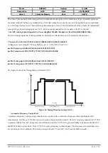
The entries from one bank of the ramp profile are partitioned into two parts, with 8 values in each part. In normal operation,
the entries in the left half part are multiplied by a 10-bit left scaling factor, and the entries in the right half part are multiplied
by a 10-bit right scaling factor. Those values are then truncated to form 16 10-bit intermediate values. Finally the intermediate
ramp profile are linearly interpolated into 32 10-bit values and sequentially used to update to the D/A converter.
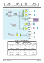
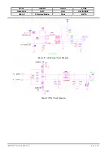
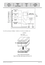
The APC Analog Signal is inputted to Power Amplifier Module through Low Pass filter (R400,R401,C406)
The APC Analog Signal has 32 Ramp profiles for Up Ramp and Down Ramp each 16 profiles as shown below.
TX power level=44,53,62,74,90,110,136,165,200,240,295,350,420,525,610,610
(Voltage Level according to TX Power GSM Level 19 ~ 5. DCS/PCS Level 15~0)
profile 0 ramp up=0,0,0,0,0,0,2,4,8,26,65,143,228,255,255,255
profile 0 ramp down=255,255,239,197,138,78,32,10,0,0,0,0,0,0,0,0
.
.
profile 15 ramp up=0,0,0,0,0,0,0,2,4,8,26,65,143,219,250,255
profile 15 ramp down=255,239,197,138,78,32,10,0,0,0,0,0,0,0,0,0
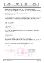
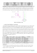
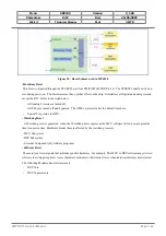
The Figure 36 shows the Timing Mask for Normal VAPC.
Figure 36. Timing Mask for normal VAPC.
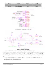
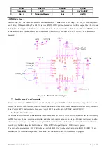
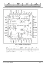
Automatic Frequency Control Unit
Automatic Frequency Control unit provides the direct control of the oscillator for frequency offset and Doppler shift
compensation. It utilizes a 13-bit D/A converter to achieve high-resolution control. The AFC is always inputted to VCTCXO
to generate 26Mhz. The AFC Voltage must be calibrated to tune the VCTCXO to generate 26Mhz to be entered the MT6120
and MT6228 Main system clock. If the VCTCXO output a frequency with much ppm , The Frequency error and Phase error
are out of range. After calibrated, The Analog voltage is about 1.5V and AFC_DAC is about 4200 decimally.
SDP100
T
ECHNICAL
M
ANUAL
Page 3.46