


2010-06-30
Page 9 of 42
IT430_Tech_doc.doc
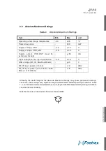
2
SPECIFICATIONS
2.1
General
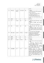
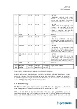
Table 1
General Specifications
Receiver
GPS L1 C/A-code, SPS
Chip set & Tracking sensitivity
SiRF IV, GSD4e, -163 dBm
Channels
48
Update rate (default)
1 Hz max (fix rate configurable)
Supply voltage, VDD
+1.71… +1.89 V
Supply voltage ripple, VDD
54 mV(RMS) max @ f = 0… 3MHz
15 mV(RMS) max @ f > 3 MHz
Power consumption
(note 1)
56 mW
(Switcher mode)
or 68 mW
(LDO
mode)
typ. @ VDD=1.8 V
Power consumption (Hibernate
state)
36 uW typical @ 1.8 V
Antenna net gain range
0…+25 dB
Antenna bias voltage VDD_ANT
+/- 5.5 V (externally generated)
Antenna bias current VDD_ANT
70 mA rated max
Storage temperature
-40ºC…+85ºC
Operating temperature
-40ºC…+85ºC (
note 2
)
Host port configuration
SPI (default), UART or I
2
C
Serial port protocol (UART)
NMEA (configurable to SiRF binary OSP)
Serial data format (UART)
8 bits, no parity, 1 stop bit
Serial data speed (UART)
4800 baud (configurable)
I/O signal levels
CMOS compatible: low state 0… +0.4 V max;
high state 0.75…1.0xVDD. Inputs are 3.6 V
tolerable
I/O output sink/source capability
+/- 2 mA max
I/O input leakage
+/- 10 uA max
TM output (1PPS)
200ms high pulse, rising edge +/-1 us
accuracy
Note 1
: Module boots for internal 1.2V LDO regulator mode. Internal Switcher mode
regulator reduces power consumption and requires a binary command from host to enable
Switcher mode, see chapter 4.2.
Note 2
: Operation in the temperature range –40
°
C… –30
°
C is allowed but Time-to-First-Fix
performance and tracking sensitivity may be degraded.
Summary of Contents for IT430
Page 24: ...2010 06 30 Page 24 of 42 IT430_Tech_doc doc Figure 3 Dimensions ...
Page 38: ...2010 06 30 Page 38 of 42 IT430_Tech_doc doc 7 3 Circuit drawing ...
Page 40: ...2010 06 30 Page 40 of 42 IT430_Tech_doc doc 7 6 Artwork layer 2 7 7 Artwork layer 3 ...
Page 41: ...2010 06 30 Page 41 of 42 IT430_Tech_doc doc 7 8 Artwork layer 4 Bottom ...


