


2010-06-30
Page 32 of 42
IT430_Tech_doc.doc
Routing signals directly under the module should be avoided. This area should be dedicated to
keep-out to both traces and assigned to ground plane (copper plane), except for via holes, which
can be placed close to the pad under the module. If possible, the amount of VIA holes
underneath the module should be minimized.
For a multi-layer PCB the first inner layer below the IT430 is suggested to be dedicated for the
ground plane. Below this ground layer other layers with signal traces are allowed. It is always
better to route very long signal traces in the inner layers of the PCB. In this way the trace can be
easily shielded with ground areas from above and below.
The serial resistors at the I/O should be placed very near to the IT430 module. In this way the
risk for the local oscillator leakage is minimized. For the same reason by-pass capacitors C1 and
C2 should be connected very close to the module with short traces to IO contacts and to the
ground plane. Place the GND via hole as close as possible to the capacitor.
Connect the GND soldering pads of the IT430 to ground plane with short traces (thermals) to via
holes, which are connected to the ground plane. Use preferably one via hole for each GND pad.
The RF input should be routed clearly away form other signals, this minimizes the possibility of
interference. The proper width for the 50 ohm transmission line impedance depends on the
dielectric material of the substrate and on the height between the signal trace and the first ground
plane. With FR-4 material the width of the trace shall be two times the substrate height.
A board space free of any traces should be covered with copper areas (GND). In this way, a solid
RF ground is achieved throughout the circuit board. Several via holes should be used to connect
the ground areas between different layers.
Additionally, it is important that the PCB build-up is symmetrical on both sides of the PCB core.
This can be achieved by choosing identical copper content on each layers, and adding copper
areas to route-free areas. If the circuit board is heavily asymmetric, the board may bend during
the PCB manufacturing or reflow soldering. Bending may cause soldering failures and reduce
end product reliability.
Summary of Contents for IT430
Page 24: ...2010 06 30 Page 24 of 42 IT430_Tech_doc doc Figure 3 Dimensions ...
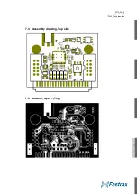
Page 38: ...2010 06 30 Page 38 of 42 IT430_Tech_doc doc 7 3 Circuit drawing ...
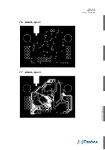
Page 40: ...2010 06 30 Page 40 of 42 IT430_Tech_doc doc 7 6 Artwork layer 2 7 7 Artwork layer 3 ...
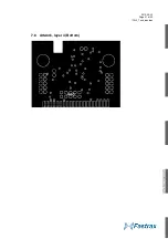
Page 41: ...2010 06 30 Page 41 of 42 IT430_Tech_doc doc 7 8 Artwork layer 4 Bottom ...


