background image

M

ODEL

 SL900A V

ERSION

 V_1.0 

P

REPARED BY

 H/W 

D

ATE

 2006.06.30 

S

UBJECT


T

ECHNICAL 

M

ANUAL


P

AGE

 44/51 


SL900A


T

ECHNICAL 

M

ANUAL                                                                                                          


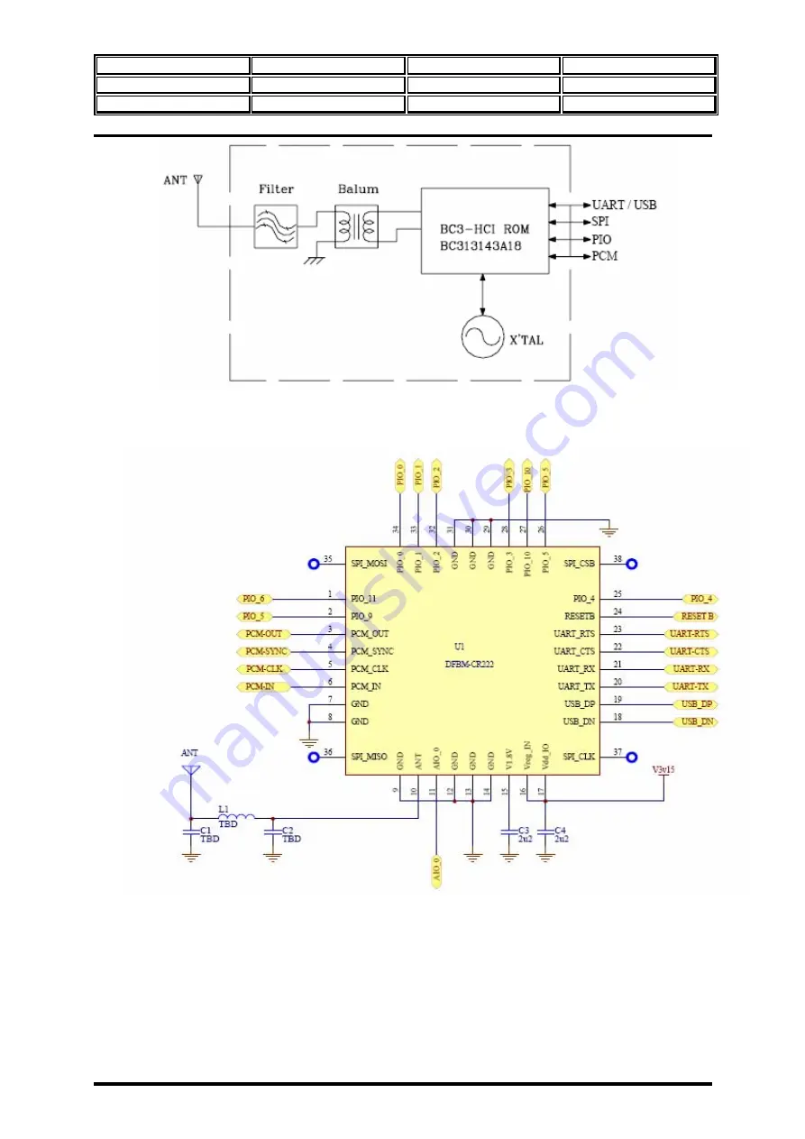
Figure 54. Block Diagram of CR222. 


Figure 55. Reference Circuit. 


The Possible Profiles are :  

HFP/HSP/FTP/OPP/DUN/SPP/A2DP/GAVDP 


Summary of Contents for SL900A

Page 1: ...SL900A SL900A ...

Page 2: ...900A Technical Manual COMPANY CONFIDENTIAL Ezze Mobile Tech Inc Tel 82 0 2 519 7700 Fax 82 0 2 519 7882 Section 1 Product Specification Contents Page SL900A specifications 1 1 Standard charger 1 4 Batteries 1 5 ...

Page 3: ...L900A Technical Manual COMPANY CONFIDENTIAL Ezze Mobile Tech Inc Tel 82 0 2 519 7700 Fax 82 0 2 519 7882 Section 2 Mechanical Construction Contents Page Disassembly 2 1 Phone disassembly 2 2 Phone Assembly 2 6 ...

Page 4: ...iption Contents Page Baseband section 3 1 MT6226M GSM GPRS Baseband processor 3 1 MT6305BN GSM Power Management System 3 20 TOME808 Mobile Multimedia Processor 3 23 PF38F3040L0ZBQ1 MCP 3 24 RF section 3 25 MT6129 RF Transceiver IC 3 25 RF3146 QUAD BAND Power Amplifier Module 3 28 LMSP54HA 348TEMP Antenna Switch Module for Tri Band 3 29 ...

Page 5: ...in out for U 109 4 4 Pin out for U 150 4 5 Pin out for CON 103 4 6 Pin out for U 601 4 7 Pin out for U 600 4 8 Pin out for U 50 4 9 Pin out for U 201 4 10 Pin out for F 100 4 12 Pin out for U 101 4 13 Pin out for U 103 4 16 Pin out for U 800 4 17 Pin out for D103 D104 D110 4 21 Pin out for D111 D116 4 22 Pin out for ZD101 ZD106 4 23 Pin out for D102 4 24 Pin out for U200 4 25 Pin out for U100 4 28...

Page 6: ...SL900A SL900A Technical Manual COMPANY CONFIDENTIAL Ezze Mobile Tech Inc Tel 82 0 2 519 7700 Fax 82 0 2 519 7882 Section 5 Spare Part List Contents Page SL900A Part List 5 1 ...

Page 7: ...g temperature 20 C to 60 C Keyboard 24 keys comprising 1 2 3 4 5 6 7 8 9 0 YES SEND NO END POWER 2 Soft Key Navigation Key Shot Key Volume Key UP DOWN Ring tones 30 user selectable tones and off Battery types Standard 500mAh Li Ion Talk time 500mAh Li Ion battery 2 3 hours approximately Standby time 500mAh Li Ion battery 140 hours approximately Note Measured on EGSM 900 with power level 5 Note Mea...

Page 8: ...display Easy text input T9 SIM application tool kit External interface connections RS232 USB Number of channels EGSM 174 Channel DCS 374 Channel PCS 299 Channels Operating frequency range transmitter EGSM TX 880MHz to 915MHz DCS TX 1710MHz to 1785MHz PCS TX 1850 MHz to 1910 MHz Operating frequency range receiver EGSM RX 925MHz to 960MHz DCS RX 1805MHz to 1880MHz PCS RX 1930 MHz to 1990 MHz ...

Page 9: ...ND Left Connector layout Pin description 1 EJ_OUT_L Cradle Audio Output 2 RXD Serial Interface RX 3 EJ_IN Cradle Enable Mic Input 4 USBPWR VCHA USB Power Input 5 USBPWR VCHA USB Power Input 6 VBAT Battery Voltage 3 8V 7 VBAT Battery Voltage 3 8V 8 EJ_OUT_R Cradle Audio Output 9 TXD Serial Interface TX 10 GND GND 11 P_ON OFF Power On Off Pin 12 USBDP USB D Input Output 13 USBDM USB D Input Output 1...

Page 10: ... out when the battery is fitted to the phone There are no serviceable parts within the main plug Input parameter Type Value Unit Input voltage min 90 V nom 230 V max 264 V Input frequency min 47 Hz nom 50 Hz max 63 Hz Input current max 200 mA Efficiency min 55 Output parameter Type Value Unit Output current CV min 0 650 A max 0 800 A CC min 0 000 A max 0 650 A Output voltage CV min 3 0 V max 4 9 V...

Page 11: ... 30dBm 2 5 hours 3 hours Charging time 1 2 hours approximately to full capacity Charge temperature 0 to 45 C Discharge temperature 20 C to 60 C Cycle life 100 cap to 80 cap 500 cycles Energy Density 344Wh I 150Wh kg Dimension W x H x L 3 6 T x 34 W x 43 L mm Weight 14 0 g Operating times depend on network and usage Variability will occur DTX 40 included Storage temperature Short period 1 month 20 ...

Page 12: ...wdriver is narrow enough to reach the screws without causing damage to the casing parts 2 The phone should always be placed on a soft surface to minimise the risk of damage being caused to the casing window and keypad If the PCB is to be removed then care should be taken not to stress or scratch the exposed LCD 3 Observe anti static precautions when handling the main PCB or any of its components 4...

Page 13: ...mbly A Pull up the lock knob in the arrow direction B Remove the battery 2 Sim card screw caps rear cover Disassembly A Remove the sim card B Remove the four caps and four screws Carefully separate the twp covers front and rear 3 Side key Caps Irda lens Disassembly A Remove the caps and side key along arrow direction ...

Page 14: ...pared by H W Date 2006 06 30 Subject Technical Manual Page 3 9 4 Main PCB Main keypad Disassembly A Separate Main PCB Assembly and Main keypad from the front cover 5 Front cover Deco rail Disassembly A From the front cover Deco rail ...

Page 15: ...Page 4 9 6 Slide unit Stopper Back cover Disassembly A Pull off the stopper from the back cover B Separate base of slide unit C Pull off the back cover from the drop cover 7 Lcd module Keypad Disassembly A Remove the Lcd module from the top cover B Remove the Keypad from the top cover ...

Page 16: ...Model SL900A Version V_1 0 Prepared by H W Date 2006 06 30 Subject Technical Manual Page 5 9 8 Lcd window Disassembly A Pull off the Lcd window from Top cover Phone Assembly ...

Page 17: ...hnical Manual Page 6 9 1 Lcd window Assembly A Group the Lcd window from Top cover 2 Lcd module Keypad Assembly A Group the Lcd module from the top cover B Group the Keypad from the top cover 3 Slide unit Stopper Back cover Assembly A Group the stopper from the back cover ...

Page 18: ...bject Technical Manual Page 7 9 B Group the slide unit C Group the back cover from the drop cover 4 Front cover Deco rail Assembly A Group the front cover Deco rail 5 Main PCB Main keypad Assembly A Group the Main PCB Assembly and Main keypad from the front cover ...

Page 19: ... V_1 0 Prepared by H W Date 2006 06 30 Subject Technical Manual Page 8 9 6 Side key Caps Irda lens Assembly A Group the caps and side key along arrow direction 9 Sim card screw caps rear cover Assembly A Group the sim card ...

Page 20: ...d by H W Date 2006 06 30 Subject Technical Manual Page 9 9 B Group the four caps and four screws Carefully separate the twp covers front and rear 10 Battery Cover Assembly A Group the lock knob in the arrow direction B Group the battery ...

Page 21: ... RF Power Amplifier RF3146 are from Media Tek Taiwan I MT6226M GSM GPRS Baseband Processor 1 System Overview The Revolutionary MT6226M is a leading edge single Chip solution for GSM GPRS mobile phones targeting the emerging applications in digital audio and video Based on 32bit ARM7EJ STM RISC processor MT6226M not only features high performance GPRS Class 12 MODEM but also provides comprehensive ...

Page 22: ... SL900A VERSION V_1 0 PREPARED BY H W DATE 2006 06 30 SUBJECT TECHNICAL MANUAL PAGE 2 51 SL900A TECHNICAL MANUAL Figure 2 is shown the Block Diagram of MT6226M for detailly Figure 2 Block Diagram of MT6226M ...

Page 23: ... TECHNICAL MANUAL PAGE 3 51 SL900A TECHNICAL MANUAL 2 Product Description 2 1 Pin Outs One type of Package for this product TFBGA 13x13mm 296balls 0 65mm pitch package is offerd Pin outs and the top view are illustrated in Figure 3 4 Figure 3 MT6226M Pin Out Top View ...

Page 24: ... VERSION V_1 0 PREPARED BY H W DATE 2006 06 30 SUBJECT TECHNICAL MANUAL PAGE 4 51 SL900A TECHNICAL MANUAL Top and Bottom View Figure 4 Top and Bottom View 2 2 Top Masking Definition Figure 5 Top masking definition ...

Page 25: ...ION V_1 0 PREPARED BY H W DATE 2006 06 30 SUBJECT TECHNICAL MANUAL PAGE 5 51 SL900A TECHNICAL MANUAL 2 3 Pin Description JTAG Port RF Parallel Control Unit RF Serial Control Unit PWM Interface Serial LCD PM IC Interface ...

Page 26: ...MODEL SL900A VERSION V_1 0 PREPARED BY H W DATE 2006 06 30 SUBJECT TECHNICAL MANUAL PAGE 6 51 SL900A TECHNICAL MANUAL Parallel LCD Nand_Flash Interface SIM Card Interface ...

Page 27: ...ODEL SL900A VERSION V_1 0 PREPARED BY H W DATE 2006 06 30 SUBJECT TECHNICAL MANUAL PAGE 7 51 SL900A TECHNICAL MANUAL Dedicated GPIO Interface Miscellaneous Key Pad Interface External Interrupt Interface ...

Page 28: ...MODEL SL900A VERSION V_1 0 PREPARED BY H W DATE 2006 06 30 SUBJECT TECHNICAL MANUAL PAGE 8 51 SL900A TECHNICAL MANUAL External Memory Interface ...

Page 29: ...MODEL SL900A VERSION V_1 0 PREPARED BY H W DATE 2006 06 30 SUBJECT TECHNICAL MANUAL PAGE 9 51 SL900A TECHNICAL MANUAL USB Interface Memory Card Interface UART Interface Digital Audio Interface ...

Page 30: ...MODEL SL900A VERSION V_1 0 PREPARED BY H W DATE 2006 06 30 SUBJECT TECHNICAL MANUAL PAGE 10 51 SL900A TECHNICAL MANUAL Image Sensor Interface Analog Interface ...

Page 31: ...MODEL SL900A VERSION V_1 0 PREPARED BY H W DATE 2006 06 30 SUBJECT TECHNICAL MANUAL PAGE 11 51 SL900A TECHNICAL MANUAL VCXO Interface RTC Interface ...

Page 32: ...MODEL SL900A VERSION V_1 0 PREPARED BY H W DATE 2006 06 30 SUBJECT TECHNICAL MANUAL PAGE 12 51 SL900A TECHNICAL MANUAL Supply Voltages ...

Page 33: ...rocessor which plays the role of the main bus master controlling the whole subsystem The processor communicates with all the other on chip modules via the two level system buses AHB Bus and APB Bus All bus transactions originate from bus masters while salves can only respond to requests from bus masters Before data transfer can be established bus master must ask for bus ownership This is accomplis...

Page 34: ...26M supports only memory addressing method for instruction fetch and data access It manages a 32bit address space that has addressing capability up to 4GB System RAM System ROM Registers MCU Peripherals and external components are all mapped onto such 32 bit address space as depicted in Figure 7 Figure 7 Memory Layout of MT6226M External Memory Access To allow external access The MT6226M outputs 2...

Page 35: ...igure the chip for factory programming The Flash downloader program is then transferred in to System RAM or external SRAM Figure 8 Factory Programming 3 3 Bus System Two levels of bus hierarchy are employed in the Micro Controller Unit Subsystem of MT6226M As depicted in Figure5 AHB Bus and APB Bus serve as system backbone and peripheral buses while an APB bridge connects these two buses Both AHB ...

Page 36: ...MODEL SL900A VERSION V_1 0 PREPARED BY H W DATE 2006 06 30 SUBJECT TECHNICAL MANUAL PAGE 16 51 SL900A TECHNICAL MANUAL ...

Page 37: ...generic DMA Controller can also be used to connect any two devices other than memory module as long as they can be addressed in memory space Figure 9 Variety data paths of DMA transfer 3 5 Interrupt Controller Figure 10 outlines the major functionality of the MCU Interrupt Controller The interrupt controller processes all interrupt sources coming from external lines and internal MCU peripherals Si...

Page 38: ...as 32bits wide with 4 byte write signals capable for byte operations Band 0 and Band 1 SRAM macros have limited repair capability The yield of SRAM is improbed if the defects inside it can be repaired uring testing System ROM The 27Kbyte System ROM is primarily used to store software program for Factory programming However due to its advantageous low latency performance some of the timing critical...

Page 39: ...face to allow the MCU access to the SIM Card It can operate via 5 terminals using SIMVCC SIMSEL SIM RST SIMCLK and SIMDATA The SIMVCC is used to control the external voltage supply to the SIM card and SIMSEL determines the regulated smart card supply voltage SIMRST is used as the SIM card reset signal Besides SIMDATA and SIMCLK are used for data exchange purpose Basically the SIM interface acts as...

Page 40: ...Purpose Timer Three general purpose timers are provided The Timers are 16 bits long and run independently of each other although they share the same clock source Two timers can opeate in ont of two modes one shot mode and auto repeat mode the other is a free running timer In ont shot mode When the timer counts down and reaches zero it is halted In auto repeat mode when the timer reaches zero it si...

Page 41: ...is empty 2 The most recent character was received longer than four character periods ago including all start parity and stop bit 3 The most recent CPU read of the FIFO was longer than four character periods ago 4 7 IrDA framer IrDA framer which is depicted in Figure 15 is implemented to reduce the CPU loading for IrDA transmission IrDA framer functional block can be divided into two parts the tran...

Page 42: ... input channels for diversified application in this unit There provides 2 modes of operation immediate mode and timer triggered mode 5 Microcontroller Coprocessors Microcontroller Coprocessors are designed to run computing intensive processes in place of the Microcontroller MCU These coprocessors especially target timing critical GSM GPRS Model processes that require fast response and large data m...

Page 43: ...are block is preferred to aid software and deal with jpeg file as much as possible As a result JPEG Decoder is designed to decode all baseline and progressive JPEG images with all YUV sampling frequencies combinations To gain the best speed performance JPEG decoder will handle all portions of JPEG files except the 17 byte SOF marker The software program only needs to program related control regist...

Page 44: ...es and 2048 2112 bytes Support 2 chip select for NAND flash parts Support 8 16bits I O Interface Support LCD Data interface together Used 7 control Signal NRE NEW NCE NALE WATCHDOG NCLE NRNB 6 5 USB Device controller MT6226M provides a USB function interface that is in compliance with Universal Serial Bus Specification Rev 1 1 The USB device controller supports only full speed 12Mbps operation The...

Page 45: ...troller The controller fully supports the SD Memory Card bus protocol as defined in SD Memory Card Specification Part1 Physical Layer Specification version1 0 But SL900A is not interfaced Mini SD card but T Flash Memory Card Interface Signals are same Normally the Detection is controlled by INS pin status When Card is nothing The INS is high logically And When Card inserted The INS is low ...

Page 46: ... imgae signal processor to connect with a variety of image sensor components This processor consists of timing generated unit TG and Lens Sensor compensation unit and image process unit So The Camera sensor doesn t need the ISP block In SL900A Camera Sensors can be selected by BB processor If MT6226M is used The Camera Module will be used 1 3Mpixels sensor from Omni OV9650 If MT6226 is used The Ca...

Page 47: ...MODEL SL900A VERSION V_1 0 PREPARED BY H W DATE 2006 06 30 SUBJECT TECHNICAL MANUAL PAGE 27 51 SL900A TECHNICAL MANUAL Figure 23 Camera Sensor Interface circuit ...

Page 48: ...quality playback external FM radio and voice playback through headset Figure 24 Audio Front End Block Diagram Figure 25 shows the block diagram of digital circuits of the audio front end The APB register block is an APB peripheral to get settings from the MCU The DSP audio port block interfaces with the DSP for control and data communications Besides there is a Digital Audio Interface DAI block to...

Page 49: ...llel Interface BPI Automatic Power Control APC and Automatic Frequency Control AFC together with APC DAC and AFC DAC 8 1 Baseband Serial Interface The Baseband Serial Interface controls external radio components A 3 wire serial bus transfers data to RF circuitry for PLL frequency change reception gain setting and other radio control purposes In this unit BSI data registers are double buffered in t...

Page 50: ...seband Parallel Interface The Baseband Parallel Interface features a 10 pin output bus used for timing critical control of the external circuits These pins are typically used to control front end components at the specified time along the GSM time base such as transmit enable PA_EN band switching BANDSW_DCS TR switch LB_TX HB_TX etc Figure 27 Baseband Parallel Interface Block Diagram ...

Page 51: ... banks of ramp profiles are used in one frame to make up 4 consecutive transmission slots The shape and magnitude of the ramp profiles are configurable to fit ramp up intermediate ramp and ramp down profiles Each bank of the ramp profile consists of 16 8 bit unsigned values which is adjustable for different conditions The entries from one bank of the ramp profile are partitioned into two parts wit...

Page 52: ...C_DAC is about 4200 decimally Figure 30 Block diagram of the AFC Controller 9 Baseband Front End Baseband Front End is a modem interface between Tx Rx mixed signal modules and digital signal processor We can divide this block into two parts The first is the uplink transmitting path which converts bit stream from DSP into digital in phase and quadrature signals for TX mixed signal module The second...

Page 53: ...plink Figure 31 Block Diagram of Baseband Front End 9 1 Baseband Serial Ports Baseband Front End communicates with DSP through the sub block of Baseband Serial Ports Baseband Serial Ports interfaces with DSP in serial manner It implies that DSP must be configured carefully in order to have Baseband Serial Ports cooperate with DSP core correctly 9 2 Downlink Path RX Path On downlink path the sub bl...

Page 54: ...of uplink parts of Baseband Serial Ports GSM Encryptor GMSK Modulator and Offset Cancellation Figure 33 Block Diagram of TX Path 10 Timing Generator Timing is the most critical issue in GSM GPRS applications The TDMA timer provides a simple interface for the MCU to program all the timing related events for receive event control transmit event control and the timing adjustment In pause mode the 13M...

Page 55: ...brate the 32Khz crystal taking the accurate 13Mhz source as the reference Figure 21 Figure 35 The Block Diagram of Slow Clocking unit 11 Power Clocks and Reset This Chapter descripbes about the power clock and reset management functions provided by MT6226M Together with Power Management IC MT6226M offers both fine and coarse resolutions of power control by way of software programming With this eff...

Page 56: ...ne is the 13MHz clock origination from an off chip temperature compensated voltage controlled oscillator that can be 26MHz This signal is the input from the SYSCLK pad then is converted to the square wave signal The other time base is the 32 768KHz clock generated by an on chip oscillator connected to an external crystal Figure 37 Clock distributions in the MT6226M 32 768Khz Time Base The 32 768Kh...

Page 57: ...ip It initializes all digital and analog circuits except the RTC Refer to the listed below All Analog Circuits are turned off All PLLs are turned off and bypassed The 13Mhz system clock is the default time base Special Trap statue in GPIO Watchdog Reset A Watchdog reset is generated when the Watchdog timer expires as the MCU software failed to re program the timer counter in time Hardware blocks t...

Page 58: ...Management System The MT6305BN is a power management system chip optimized for GSM handsets especially those based on the MTK system solution It contains seven LDOs one to power each of the critical GSM sub blocks Sophisticated controls are available for power up during battery charging keypad interface and RTC alarm The interface Features are listed below Handles all GSM baseband Power management...

Page 59: ... regulator that could source 100mA with 1 2V output voltage with Pin3 DANODE GND If Pin2 is not GND The output Voltage is 1 8V It supplies the baseband circuitry in the handset The LDO is optimized for very low quiescent current 3 Digital IO LDO DVDD The digital IO LDO is a regulator that could source 100mA with 2 8V output voltage It supplies the baseband circuitry in the handset 4 Analog LDO AVD...

Page 60: ...he memory LDO is a regulator that could source 150mA with 1 8V or 2 8V output voltage selection based on the supply specs of memory chips It supplies the memory circuitry in the handset 8 SIM LDO Vsim The SIM LDO is a regulator that could source 20mA with 1 8V or 3 0V output voltage selection based on the supply specs of subscriber identity modules card The LDO is controlled independently of the o...

Page 61: ... VIBRATOR pin is dedicated to Vibrator Motor 11 Battery Charger BATUSE pin can set MT6305 to fit the battery type When BATUSE is set low Li ion battery is used MT6305 charges the battery in three phases pre charging constant current mode charging and constant voltage mode charging The circuitry of MT6305 combines with a PMOS transistor diode current sense resistor externally to form a simple and l...

Page 62: ...al format IV Blue Tooth CR222 The Blue Tooth Module CR222 is a class 2 module compliant with Bluetooth TM Specification V1 2 with CSR BC3 chip The Features are followings Suitable for Cellular Phones PDA Digital Cameras Support for 802 11 coexistence Small size and Low profile using high density packaging technology High sensitivity for better reception Various interfaces UART USB PIO and PCM Wide...

Page 63: ...MODEL SL900A VERSION V_1 0 PREPARED BY H W DATE 2006 06 30 SUBJECT TECHNICAL MANUAL PAGE 43 51 SL900A TECHNICAL MANUAL The Figure 54 is shown the block diagram of CR222 ...

Page 64: ...N V_1 0 PREPARED BY H W DATE 2006 06 30 SUBJECT TECHNICAL MANUAL PAGE 44 51 SL900A TECHNICAL MANUAL Figure 54 Block Diagram of CR222 Figure 55 Reference Circuit The Possible Profiles are HFP HSP FTP OPP DUN SPP A2DP GAVDP ...

Page 65: ...t smart combo RAM and a 128Mbit Flash memory The BYTE inputs can be used to select the optimal memory configuration The power supply for the PF38F3040L0ZBQ1 can range from 1 7V to 1 95V The PF38F3040L0ZBQ1 can perform simultaneous read write operations on its flash memory and is available in a 88 pin BGA package making it suitable for a variety of applications The Boot block architecture for flash...

Page 66: ...cludes LNAs two RF quadrature mixers an integrated channel filter programmable gain amplifiers PGA an IQ demodulator for the receiver a precision IQ modulator with offset PLL for the transmitter two internal TX VCOs a VCXO on chip regulators and a fully programmable sigma delta fractional N synthesizer with an on chip RF VCO Figure 30 MT6129 Functional block diagram ...

Page 67: ...he adjacent channel interference performance The SL900A was designed for Tri Band GSM900 DCS1800 PCS1900 Receiver Input Frequency Mode Min Max Unit GSM900 925 960 Mhz DCS 1805 1880 Mhz PCS 1930 1990 Mhz 2 Transmitter The MT6120 transmitter section consists of two on chip TX VCOs buffer amplifiers a down converting mixer a quadrature modulator an analog phase detector and a digital phase frequency ...

Page 68: ...alibration a fast acquisition system is utilized for a period of time to facilitate fast locking The frequency ranges of the synthesizer for RX mode are RX mode GSM850 1737Mhz 1788Mhz E GSM900 1850Mhz 1920Mhz DCS1800 1805Mhz 1880Mhz PCS1900 1930Mhz 1990Mhz The Calculate LO Freqnecy Fvco from RX Channel Frequency Fch is following Fvco 2 Fch 200K for GSM850 and E GSM900 Fvco Fch 100K for DCS1800 and...

Page 69: ...nance with a standard 26Mhz crysatal The Crystal is connected from the Input pin XAL of Amplifier to ground through a series load capacitance The buffer provides a typical 600mVpp voltage swing As an alternative the reference frequency can ve provided by an external 26Mhz VCTCXO module When Pin VCXOCXR is tied to the VCCVCXO supply the XTAL pin will accept an external signal Furthermore the VCXO c...

Page 70: ...iminating the need for directional couplers detector diodes power control ASICs and other power control circuitry See figure 34 this allows the module to be driven directly from the DAC output The device is designed for use as the final RF amplifier in EGSM900 and DCS handsets On board power control provides over 50dB of control range with an analog voltage input The RF3146 has Max 35dBm GSM outpu...

Page 71: ...ltage for the second and third stages are regulated to the multiplied Vramp voltage The basic circuit is shown as above III LMSP54HA 348TEMP Antenna Switch Module for Tri Band with SAW Filter LMSP54HA 348TEMP is an Antenna Switch Module for GSM900 DCS1800 and PCS1900 of Murata with Three SAW Modules Control Pins VC1 VC2 VC3 are connected to LB_TX HB_TX PCB signals from baseband processor The Contr...

Page 72: ...Page 1 Pin out for U204 LMSP54HA 348TEMP PIN NO FUNCTION NAME 1 2 3 4 5 6 7 8 9 10 11 12 13 14 GSM900 RX1 GSM900 RX2 DCS1800 RX1 DCS1800 RX2 PCS1900 RX1 PCS1900 RX2 GND DCS PCS TX VC2 GSM TX VC1 VC3 ANT GND GSM900 RX1 GSM900 RX2 DCS1800 RX1 DCS1800 RX2 PCS1900 RX1 PCS1900 RX2 GND DCS PCS TX VC2 GSM TX VC1 VC3 ANT GND ...

Page 73: ...Model SL900 Version V_1 0 Prepared by H W Date 2006 06 30 Subject Technical Manual Page 2 41 SL900 Technical Manual Page 2 Pin out for U203 CSX 325T26BADT J2E ...

Page 74: ...Model SL900 Version V_1 0 Prepared by H W Date 2006 06 30 Subject Technical Manual Page 3 41 SL900 Technical Manual Page 3 Pin out for BAT100 TS414H I106E PIN NO FUNCTION NAME 1 2 VCC Ground VCC GND ...

Page 75: ...06 06 30 Subject Technical Manual Page 4 41 SL900 Technical Manual Page 4 Pin out for U109 HSDL 3208 PIN NO FUNCTION NAME 1 2 3 4 5 6 7 LED ANODE LED CATHODE TRANSMIT DATA RECEIVE DATA SHUTDOWN SUPPLY VOLTAGE GROUND LED A LED C TXD RXD SD MODE VCC GND ...

Page 76: ...Model SL900 Version V_1 0 Prepared by H W Date 2006 06 30 Subject Technical Manual Page 5 41 SL900 Technical Manual Page 5 Pin out for U150 DF30FC 40DS 0 4V ...

Page 77: ...y H W Date 2006 06 30 Subject Technical Manual Page 6 41 SL900 Technical Manual Page 6 Pin out for CN103 SCHB1A0101 PIN NO FUNCTION NAME 1 2 3 4 5 6 7 8 MCDA2 MCDA3 MCCMO VCC MCCK GROUND MCDA0 MCDA1 DAT2 CD DAT3 CMD VDD CLK VSS DAT0 DAT1 ...

Page 78: ...2006 06 30 Subject Technical Manual Page 7 41 SL900 Technical Manual Page 7 Pin out for U601 A3212EEHLT PIN NO FUNCTION NAME 1 2 3 4 5 6 Output No connection GND GND No connection Power supply OUTPUT NO CONNECTION GROUND GROUND NO CONNECTION SUPPLY ...

Page 79: ...red by H W Date 2006 06 30 Subject Technical Manual Page 8 41 SL900 Technical Manual Page 8 Pin out for U600 TS4990IJT PIN NO FUNCTION NAME 1 2 3 4 5 6 7 8 9 IN GROUND BYPASS V02 SHUTDOWN VDD IN V01 GROUND A1 B1 C1 C2 C3 B3 A3 A2 B2 ...

Page 80: ... Date 2006 06 30 Subject Technical Manual Page 9 41 SL900 Technical Manual Page 9 Pin out for U50 XC6401EE20MR PIN NO FUNCTION NAME 1 2 3 4 5 6 ON OFF Control 1 Power Input ON OFF Control 2 Output 2 Ground Output 1 EN1 VIN EN2 VOUT2 VSS VOUT1 ...

Page 81: ...Model SL900 Version V_1 0 Prepared by H W Date 2006 06 30 Subject Technical Manual Page 10 41 SL900 Technical Manual Page 10 Pin out for U201 RF3146 ...

Page 82: ...ed VCC2 and VCC3 Controlled voltage input to the DCS PCS output stage Internal circuit node Do not externally connect Internal circuit node Do not externally connect No Internal or external connection Internal circuit node Do not externally connect Internal circuit node Do not externally connect Internal circuit node Do not externally connect Internal circuit node Do not externally connect Interna...

Page 83: ...Model SL900 Version V_1 0 Prepared by H W Date 2006 06 30 Subject Technical Manual Page 12 41 SL900 Technical Manual Page 12 Pin out for F100 0467 001 NR ...

Page 84: ...9 4 5 6 7 8 9 10 Charger Input Voltage Gate Drive Output No Connect Charger Current Sense Input Microprocessor Control Input Signal for Gate Drive Internal Pull Low to DGND Charger Detect Output Battery Input Voltage Sense SIM Supply Non Level Shifted Bidirectional Data I O Non Level Shifted SIM Reset Input Internal CHRIN GATEDRV NC ISENSE CHRCNTL CHRDET BATSNS VSIM SIMIO SIMRST ...

Page 85: ...ircuits Analog Supply Analog Ground Referenced Voltage Output VTCXO and VA Enable Power on off Key Internal Pull High to VBAT Power on off Signal from Microprocessor Vibrator Driver Enable Internal Pull Low to DGND Alerter Driver Enable Internal Pull Low to DGND LED Driver Enable Internal Pull Low to DGND Power Ground Vibrator Driver Input Alerter Driver Input LED Driver Input Battery Type Selecti...

Page 86: ...Version V_1 0 Prepared by H W Date 2006 06 30 Subject Technical Manual Page 15 41 SL900 Technical Manual Page 15 High for Vm 2 8V Low for Vm 1 8V Internal Pull High to VIO Battery Input Voltage Digital Core Supply ...

Page 87: ... Prepared by H W Date 2006 06 30 Subject Technical Manual Page 16 41 SL900 Technical Manual Page 16 Pin out for U103 AO8701 PIN NO FUNCTION NAME 1 2 3 4 5 6 7 8 Drain Source Source Gate Cathode Anode Anode Anode D S S G K A A A ...

Page 88: ...Model SL900 Version V_1 0 Prepared by H W Date 2006 06 30 Subject Technical Manual Page 17 41 SL900 Technical Manual Page 17 Pin out for U800 PF38F3040L0ZBQ1 ...

Page 89: ...Model SL900 Version V_1 0 Prepared by H W Date 2006 06 30 Subject Technical Manual Page 18 41 SL900 Technical Manual Page 18 ...

Page 90: ...Model SL900 Version V_1 0 Prepared by H W Date 2006 06 30 Subject Technical Manual Page 19 41 SL900 Technical Manual Page 19 ...

Page 91: ...Model SL900 Version V_1 0 Prepared by H W Date 2006 06 30 Subject Technical Manual Page 20 41 SL900 Technical Manual Page 20 ...

Page 92: ...odel SL900 Version V_1 0 Prepared by H W Date 2006 06 30 Subject Technical Manual Page 21 41 SL900 Technical Manual Page 21 Pin out for D103 D104 D110 RB520S 30 PIN NO FUNCTION NAME 1 2 Anode Cathode A C ...

Page 93: ...Model SL900 Version V_1 0 Prepared by H W Date 2006 06 30 Subject Technical Manual Page 22 41 SL900 Technical Manual Page 22 Pin out for D111 D116 SSC HB103 69 PIN NO FUNCTION NAME 1 2 Anode Cathode A C ...

Page 94: ...900 Version V_1 0 Prepared by H W Date 2006 06 30 Subject Technical Manual Page 23 41 SL900 Technical Manual Page 23 Pin out for ZD101 106 AVRC5S05Q050 100R PIN NO FUNCTION 1 3 5 7 2 4 6 8 9 Input Output Ground ...

Page 95: ...Model SL900 Version V_1 0 Prepared by H W Date 2006 06 30 Subject Technical Manual Page 24 41 SL900 Technical Manual Page 24 Pin out for D102 PG12HSUSC PIN NO FUNCTION NAME 1 2 Anode Cathode A C ...

Page 96: ...ical Manual Page 25 Pin out for U200 MT6129 PIN NO FUNCTION NAME 1 2 3 4 TX VCO supply voltage and Regulator 1 TX VCO voltage output Regulator 1 external noise bypass capacitor Battery supply for Regulator1 TRX RF and TX BUF block supply voltage and Regulator 1 TRX voltage output VCCTXVCO CREG1 VBAT1 VCCRF ...

Page 97: ...Battery supply for Regulator 2 RF VCO buffer supply voltage and Regulator 2 SX voltage output RFVCO buffer ground RF VCO differential positive test output RF VCO ground Loop filter main capacitor input RF VCO supply voltage and Regulator RF VCO voltage output Synthesizer charge pump and PFD ground NC Synthesizer charge pump and PFD supply voltage Synthesizer supply voltage Synthesizer ground VCXO ...

Page 98: ...ut 3 wire serial bus clock input 3 wire serial bus data input Auxiliary test output Q path negative baseband input output Q path positive baseband input output I path negative baseband input output I path positive baseband input output IF circuit supply voltage Transmitter PFD and Receiver IF circuit supply voltage Transmitter charge pump supply voltage No connection Transmitter charge pump ground...

Page 99: ...Model SL900 Version V_1 0 Prepared by H W Date 2006 06 30 Subject Technical Manual Page 28 41 SL900 Technical Manual Page 28 Pin out for U100 MT6226M ...

Page 100: ... Version V_1 0 Prepared by H W Date 2006 06 30 Subject Technical Manual Page 29 41 SL900 Technical Manual Page 29 JTAG PORT RF PARALLEL CONTROL UNIT RF SERIAL CONTROL UNIT PWM INTERFACE SERIAL LCD PM IC INTERFACE ...

Page 101: ...Model SL900 Version V_1 0 Prepared by H W Date 2006 06 30 Subject Technical Manual Page 30 41 SL900 Technical Manual Page 30 PARALLEL LCD NAND_FLASH INTERFACE SIM CARD INTERFACE DEDICATED GPIO INTERFACE ...

Page 102: ...Model SL900 Version V_1 0 Prepared by H W Date 2006 06 30 Subject Technical Manual Page 31 41 SL900 Technical Manual Page 31 MISCELLANEOUS KEY PAD INTERFACE EXTERNAL INTERRUPT INTERFACE ...

Page 103: ...Model SL900 Version V_1 0 Prepared by H W Date 2006 06 30 Subject Technical Manual Page 32 41 SL900 Technical Manual Page 32 EXTERNAL MEMORY INTERFACE ...

Page 104: ...Model SL900 Version V_1 0 Prepared by H W Date 2006 06 30 Subject Technical Manual Page 33 41 SL900 Technical Manual Page 33 USB INTERFACE MEMORY CARD INTERFACE ...

Page 105: ...Model SL900 Version V_1 0 Prepared by H W Date 2006 06 30 Subject Technical Manual Page 34 41 SL900 Technical Manual Page 34 UART INTERFACE DIGITAL AUDIO INTERFACE IMAGE SENSOR INTERFACE ...

Page 106: ...Model SL900 Version V_1 0 Prepared by H W Date 2006 06 30 Subject Technical Manual Page 35 41 SL900 Technical Manual Page 35 ANALOG INTERFACE ...

Page 107: ...Model SL900 Version V_1 0 Prepared by H W Date 2006 06 30 Subject Technical Manual Page 36 41 SL900 Technical Manual Page 36 VCXO INTERFACE RTC INTERFACE SUPPLY VOLTAGES ...

Page 108: ...Model SL900 Version V_1 0 Prepared by H W Date 2006 06 30 Subject Technical Manual Page 37 41 SL900 Technical Manual Page 37 ...

Page 109: ...Model SL900 Version V_1 0 Prepared by H W Date 2006 06 30 Subject Technical Manual Page 38 41 SL900 Technical Manual Page 38 ANALOG SUPPLIES ...

Page 110: ...Model SL900 Version V_1 0 Prepared by H W Date 2006 06 30 Subject Technical Manual Page 39 41 SL900 Technical Manual Page 39 Pin out for U110 DFBM CR222 ...

Page 111: ...Model SL900 Version V_1 0 Prepared by H W Date 2006 06 30 Subject Technical Manual Page 40 41 SL900 Technical Manual Page 40 ...

Page 112: ...Model SL900 Version V_1 0 Prepared by H W Date 2006 06 30 Subject Technical Manual Page 41 41 SL900 Technical Manual Page 41 ...

Page 113: ...25 R226 4 220 CHIP RES 1005 1 16W 5 R141 R142 R143 R144 R155 R156 6 R650 R950 2 1K CHIP RES 1005 1 16W 5 R123 R210 R211 3 R631 R632 R633 R634 R652 5 1 5K CHIP RES 1005 1 16W 5 R118 1 3 9K CHIP RES 1005 1 16W 5 R152 1 4 7K CHIP RES 1005 1 16W 5 R653 1 R15 R34 R802 R806 R807 R809 R810 R811 8 10K CHIP RES 1005 1 16W 5 R202 R335 2 15K CHIP RES 1005 1 16W 5 R203 1 22K CHIP RES 1005 1 16W 5 R600 1 24K C...

Page 114: ...LCC 1005 X7R 10 16V C216 C256 2 0 047UF MLCC 1005 X7R 10 10V C114 1 C620 C633 C634 C654 C655 C659 C800 C801 C802 9 0 1UF MLCC 1005 Y5V 80 20 16V C103 C111 C112 C123 C124 C140 C170 C185 C187 C188 C189 C190 C224 C226 C230 C238 C246 17 0 1UF MLCC 1005 X7R 10 16V C151 1 0 47UF MLCC 1005 X5R 6 3V C180 1 C1 C2 C7 C8 C9 C16 C17 C193 C604 C29 11 1UF MLCC 1005 Y5V 80 20 6 3V C147 C150 C152 C155 C157 C158 C...

Page 115: ...LMSP54HA 348TEMP FEM U204 1 AAT3140 CHARGE PUMP U2 1 XC6401EE20MR 1 8V 2 8V LDO U50 1 XC6219B332MR 3 3V 150mA LDO U333 1 XC6219B282MR 2 8V LDO U60 1 AO8701 P MOSFET WITH DIODE U103 1 CM415DZFT J2E 32 768KHZ 32 768K Hz OSC100 1 CSX 325T26BADT J2E 26MHZ 26MHZ TCXO U203 1 ZD101 ZD102 ZD103 3 AVRC5S05Q050 100R EMI FILTER ZD104 ZD105 ZD106 3 KDR729 DIODE SCHOTTKY D601 1 RB520S 30 DIODE SCHOTTKY D103 D1...

Page 116: ...ts list for SL900A SL900A Technical Manual Page 4 4 2 Manual DESCRIPTION REFERENCE N O Q TY JND 1318PK22 SPEAKER SPK 1 MC121B 0BA4A0523 CAMERA MODULE 1 LA4 460AH VIBRATOR 1 DLC 3532WH3 10 00 FLASH LED LED300 1 FLASH LED FPCB 13 15mm 3 8mm GOLD 2L 1 SIDE FPCB 7 2mm 18mm GOLD 2L 1 CAMERA FPCB 11 5mm 6 8mm GOLD 2L 1 ...

Reviews: