background image

5

CIRCUIT DIAGRAMS

179 

/ 266

Art. No. 801

16-201

0

9

 / 200

4

ICC 200, 300, 350

CPU PCB
30128-052

2

Diese Zeichnung

ist urheber-

ohne unsere Genehmigung

Benennung/Title

Zeichnungsnummer/DWG.NO

Gert/UNIT

Weitergabe und Vervielfltigung

rechtlich gesch

tzt,

daher

unzulssig

Datum

Name

Gezeich.

Gepr

ft

LP un.:

LP bs.:

Blatt

von

Datum

Name

nderung

Nr.

M.Fritz

ICC

CPU

3

30128-052

30128-052

40128-026

29.07.92

B

C13

+

15uF

C14

+

15uF

C16

180nF

C17

180nF

C18

180nF

C19

1nF

C20

68nF

D1

1N4148

D7

D6

D5

D4

D3

D2

D1

D0

A0

A1

RD

RDY

CS

AIN1

AIN2

AIN3

AIN4

VREF+

VREF-

A

D

6

7

8

9

17

18

19

20

IC14

AD7824

&

74HC00

IC11

&

74HC00

IC11

20

19

40

39

38

D0

D1

D2

D3

D4

D5

D6

D7

B/A SEL

C/D SEL

CE

M1

IORQ

INT

IEI

IEO

A0

A1

A2

A3

A4

A5

A6

A7

ARDY

ASTB

B0

B1

B2

B3

B4

B5

B6

B7

BRDY

BSTB

1

3

2

RD

CLK

Z80PIO

IC4

20

19

40

39

38

D0

D1

D2

D3

D4

D5

D6

D7

B/A SEL

C/D SEL

CE

M1

IORQ

INT

IEI

IEO

A0

A1

A2

A3

A4

A5

A6

A7

ARDY

ASTB

B0

B1

B2

B3

B4

B5

B6

B7

BRDY

BSTB

1

3

2

RD

CLK

Z80PIO

IC5

20

19

40

39

38

D0

D1

D2

D3

D4

D5

D6

D7

B/A SEL

C/D SEL

CE

M1

IORQ

INT

IEI

IEO

A0

A1

A2

A3

A4

A5

A6

A7

ARDY

ASTB

B0

B1

B2

B3

B4

B5

B6

B7

BRDY

BSTB

1

3

2

RD

CLK

Z80PIO

IC6

20

19

40

39

38

D0

D1

D2

D3

D4

D5

D6

D7

B/A SEL

C/D SEL

CE

M1

IORQ

INT

IEI

IEO

A0

A1

A2

A3

A4

A5

A6

A7

ARDY

ASTB

B0

B1

B2

B3

B4

B5

B6

B7

BRDY

BSTB

1

3

2

RD

CLK

Z80PIO

IC7

R15

1k

R16

1k

R17

1k

R18

1k

R7

680k

R8

5M6

R9

22k

RN1

8*1k

CS4

CS5

CS6

CS7

CS8

INT

INT

INT

INT

IORQ

IORQ

IORQ

IORQ

M1

RD

RD

RD

RD

RD

RES

SICHER

WAIT

ABUS

ABUS

CLK

CLK

CLK

CLK

DBUS

DBUS

FISCH-A1

FISCH-A2

FISCH-A3

FISCH-B1

FISCH-B2

FISCH-B3

FUSS-A1

FUSS-A2

FUSS-B1

FUSS-B2

GND

GND

GND

GND

GND

GND

GNDGND

GNDGND

GNDGND

GND

IEI_5

IEI_5

IEI_6

IEI_6

IEI_7

IEI_7

J1/10

J1/11

J1/12

J1/13

J1/14

J1/15

J1/16

J1/17

J1/18

J1/19

J1/21

J1/22

J1/24

J1/25

J1/26

J1/27

J1/28

J1/29

J1/30

J1/31

J1/32

J1/33

J1/34

J1/35

J1/8

J1/9

J2/13C

J2/18C

J2/19C

J2/20C

J2/23A

J2/24A

J2/24C

J2/25A

J2/25C

J2/26A

J2/26C

J2/27A

J2/27C

J2/28A

J2/28C

J2/29A

J2/29C

J2/30A

J2/30C

J2/31C

J2/6A

J2/6C

J2/7A

J2/7C

J2/8A

J2/8C

J2/9A

M1_PIO

M1_PIO

M1_PIO

M1_PIO

M1_PIO

MC-FREI

PIC-RTCC

Vcc

+5V

Vcc

+5V

Vcc

+5V

Vcc

+5V

WDI

A1

A0

A0

A1

A1

A0

A1

A0

A0

A1

16

10

22

21

4

3

2

1

D0-D7

15

14

13

9

10

8

12

13

11

10

12

13

14

15

16

17

18

21

22

23

24

25

27

28

29

30

31

32

33

34

35

36

37

4

5

6

7

8

9

D0-D7

10

12

13

14

15

16

17

18

21

22

23

24

25

27

28

29

30

31

32

33

34

35

36

37

4

5

6

7

8

9

D0-D7

10

12

13

14

15

16

17

18

21

22

23

24

25

27

28

29

30

31

32

33

34

35

36

37

4

5

6

7

8

9

D0-D7

10

12

13

14

15

16

17

18

21

22

23

24

25

27

28

29

30

31

32

33

34

35

36

37

4

5

6

7

8

9

D0-D7

1

5

4

3

2

9

8

7

6

Summary of Contents for ICC 200

Page 1: ...Service manual ERBE ICC 200 ICC 300 H E ICC 350 09 2004...

Page 2: ......

Page 3: ...8 054 10128 055 10128 056 10128 058 10128 061 10128 064 10128 065 10128 066 10128 070 10128 071 10128 072 10128 073 10128 074 10128 075 10128 076 10128 077 10128 078 10128 080 10128 081 10128 082 1012...

Page 4: ...be revised or extended without prior notice and represents no obligation on the part of ERBE Elektromedizin GmbH Copyright ERBE Elektromedizin GmbH T bingen 2004 Printed by ERBE Elektromedizin GmbH T...

Page 5: ...nit 15 Front panel of the ICC 350 after starting up the unit 16 Test programs 1 8 17 Test program 9 Display programs 1 12 28 Test programs 10 15 39 Test program 16 Adjustments measuring equipment jump...

Page 6: ...6 266...

Page 7: ...Chapter1 Test programs and adjustments...

Page 8: ......

Page 9: ...x 7 NESSY Version number setting x 8 Display of software version no and option no x 9 Activation of display programs x 10 Time limit setup x 11 Measurement and display of extra low voltages 15 volts...

Page 10: ...UTO COAG and AUTO BIPOLAR control panels apply to the ICC 300 Calling up Press key 3 Roll when switching on the power and hold it down Setting the test program number Using keys 8 Up or 9 Down set the...

Page 11: ...350 ICC 300 Autostart stage Basic settings Remarks 0 0 s adjustable using Test program 23 1 0 5 s 2 1 s AUTO START delay ICC 200 no stepping 0 5 s Time limit setting ICC 350 output max time limit Tes...

Page 12: ...a r p S x a m s t t a w 0 6 g n i t t e s h c t i w s t o o F T U C O T U A w o l l e y G A O C O T U A e u l b h t i w 0 0 2 C C I g n i t t e s c i s a B n o i t p o T U C O D N E T U C O T U A 3 t...

Page 13: ...rting up the unit Factory programming g n i m m a r g o r p c i s a B n o i t p o T U C O D N E t u o h t i w 0 0 2 C C I T U C O T U A 3 t c e f f E x a m s t t a w 0 2 1 G A O C O T U A D E C R O F...

Page 14: ...C I T U C O T U A 3 t c e f f E x a m s t t a w 0 0 2 G A O C O T U A D E C R O F x a m s t t a w 5 2 G A O C O T U A T F O S x a m s t t a w 5 6 G A O C O T U A R A L O P I B x a m s t t a w 0 2 y l...

Page 15: ...01 09 2004 Front panel of the ICC 300 After starting up the unit Factory setting Basic setting ICC 300 AUTO CUT Effect 3 150 watts max AUTO COAG SOFT 60 watts max AUTO BIPOLAR AUTO START off 60 watts...

Page 16: ...ing up the unit Factory setting Basic setting ICC 350 AUTO CUT Effect 3 150 watts max HIGH CUT switched off AUTO COAG 1 SOFT 60 watts max AUTO COAG 2 FORCED 60 watts max AUTO BIPOLAR AUTO START off AU...

Page 17: ...lay is set the seven segment display changes to This means that the channel has been switched off Basic setting and brief power failure For a brief power failure of 15 seconds max the front panel sett...

Page 18: ...ERROR numbers The most recent error occurring chronologically is in memory location 1 Display AUTO CUT AUTO COAG 1 AUTO COAG 2 AUTO BIPOLAR Err 1 10 xxx xxx Display of the error number By pressing key...

Page 19: ...nes d0 d7 The signal lines d0 d7 are switched on and off one after another The switching statuses can be displayed on the bar graph adapter board 30183 102 Using the keys 8 Up or 9 Down you can call u...

Page 20: ...Motherboard 3 D FF IC 9 Extra low voltage and tone 4 D FF IC 19 Control board 5 D FF IC 20 Control board 6 D FF IC 6 ST power stage 7 D FF IC 10 Senso board 8 D FF IC 8 Relay board not ICC 200 9 Exten...

Page 21: ...optical signals on the front panel General description Using this program you can test the optical displays on the front panel After starting the test program you will see the following display All op...

Page 22: ...applies between the test numbers and the sounds Test no Tones switched on Tone variants Remarks 0 Tone generation switched off 1 Basic tone 1 Volume adjustable 2 Basic tone 2 Volume adjustable 3 Basic...

Page 23: ...am no 5 Activate Test program no 5 MP 4 is GND for frequency counter Call Tone 1 Set frequency at MP 1 with TP 2 to 493 Hz 2 Hz with frequency counter Call Tone 2 Set frequency at MP 2 with TP 3 to 41...

Page 24: ...e test program you will see the following display Display AUTO CUT AUTO COAG 1 AUTO COAG 2 AUTO BIPOLAR rEL 0 1 Designation of the PCBs with their assigned relays PCB Slot Relay function Remarks Mothe...

Page 25: ...nt limitation all other relays switched off Test no 1 Switch on all relays Test object Relay status Remarks Rel 1 motherboard switched on Power starting current limitation Rel 2 motherboard depending...

Page 26: ...9 Down you can set four different NESSY versions No AUTO CUT AUTO COAG 1 Remarks 1 NE 1 or for split and non split electrodes 2 NE 2 only for non split electrodes 3 NE 3 only for split electrodes aco...

Page 27: ...entification number After starting the program you will see the following display Display AUTO CUT AUTO COAG 1 AUTO COAG 2 AUTO BIPOLAR Snr x xx y Explanation x xx Software version no e g 2 0 y Option...

Page 28: ...isplay AUTO CUT AUTO COAG 1 AUTO COAG 2 AUTO BIPOLAR nr 0 Within Test program no 9 22 subprograms for displaying specific data can be called up while subprograms 16 to 22 are intended only for use by...

Page 29: ...hed back on again Display program no 1 not assigned Display program no 2 not assigned Display program no 3 ST generator time control with activation of SPRAY or FORCED Display for ICC 350 and ICC 300...

Page 30: ...surement Display program no 4 ST generator measurement values with ST generator activation FORCED activation Display for ICC 200 AUTO CUT AUTO COAG uuu USt uuu Measurement value of the output voltage...

Page 31: ...it voltage Display program no 6 ST generator measurement values for ST generator activation FORCED activation Measurement value Ist Display for ICC 200 AUTO CUT AUTO COAG iii Ist iii Measurement value...

Page 32: ...p HF power output W present power output uuu HF output voltage V present output voltage cos cos j value from the table ICC 350 only PU Abbreviation of the test title Power and voltage measurement Disp...

Page 33: ...the measurement value from the HF output current cos cos j value from the table ICC 350 only ppp HF power output W for ICC 350 IC Abbreviation of the test title Current measurement and cos j measureme...

Page 34: ...UTO CUT AUTO COAG uuu U uuu HF output voltage V U Abbreviation of the test title Voltage measurement Display program no 11 Measurement values for activation of the sine wave generator AUTO CUT AUTO CO...

Page 35: ...P3 br uuu Measurement value of the contact monitor voltage measurement P2 Set power for AUTO COAG 1 W P3 Set power for AUTO COAG 2 W br Contact monitor Display program no 12 Contact resistance for AU...

Page 36: ...by operation Display for ICC 200 AUTO CUT AUTO COAG uuu br uuu Measurement value of the contact monitor voltage measurement br Contact monitor Display program no 12 Contact resistance for AUTO START i...

Page 37: ...COAG 1 AUTO COAG 2 AUTO BIPOLAR rtr P2 P3 br rtr calculated NESSY transition resistance Ohm P2 set power for AUTO COAG 1 W P3 set power for AUTO COAG 2 W br AUTO START monitor Display program no 15 NE...

Page 38: ...1 TEST PROGRAMS AND ADJUSTMENTS 38 266 NOTE Display programs nos 13 and 14 are not assigned The program nos 17 22 are only intended for internal use by the manufacturer Display programs nos 13 22...

Page 39: ...using the appropriate Up or Down key After termination of Test program 10 using key 3 the settings made are stored In case of memory failure as well as in the delivery condition the max time limit fo...

Page 40: ...G 2 AUTO BIPOLAR U 0 XX X U 1 XX X U 2 XX X tPt ttt xxx Ch 4 22 yyy XX X Voltage value V ttt Temperature C xxx ADC measurement value in the range 0 255 yyy ADC measurement value in the range 0 255 Usi...

Page 41: ...5 Measurement and display of the supply voltage controlled to 15 volts Display XX X e g 14 6 equals 14 6 volts Voltage test U 1 or 15 Measurement and display of the supply voltage controlled to 15 vol...

Page 42: ...1 TEST PROGRAMS AND ADJUSTMENTS 42 266...

Page 43: ...V2 0 or 1 4 V4 0 Call up the version number using the Up 8 or Down 9 keys Forced version vs nr 1 A power limitation of 1 to 30 watts increases the no load voltage constantly up to approx 1 300 Vp Abo...

Page 44: ...n see vs nr 2 possible via arc FORCED voltage version vs nr 4 A power limitation of 1 to 30 watts increases the no load voltage constantly up to approx 2 600 Vp Above 30 watts power limitation the no...

Page 45: ...ection containers in completely discharged condition i e after use Otherwise care must be taken to prevent shorting in accordance with the battery regulations Test program no 16 Pre information Recomm...

Page 46: ...hese jumpers are already positioned during production and must never be changed randomly For a software update make certain that the jumpers are correctly plugged in Back up plugs are in the bag with...

Page 47: ...nation see following explanation The J5 and J6 slots are read by the CPU as a binary number In this way four different functioning methods independent from one another are programmable by plugging in...

Page 48: ...ially applies to the USA ERROR 30 warning appears due to delivery status not USA ERROR 30 deactivated here Regardless of the selection special settings are necessary for specific countries These can b...

Page 49: ...ERROR 30 In addition there are large area coagulation forceps for which a resistance less than 50 ohms is set insofar as the legs are only open to a small degree If the operating surgeon activates su...

Page 50: ...ure lasts longer than 15 seconds the test program is no longer automatically called up This text describes only the function of the program The unit is adjusted according to the adjustment instruction...

Page 51: ...of the power supply unit 3 Setting of the actuation pulse length for the HF generator 4 Phase relationship of the HF generator 5 Current voltage setting of the HF generator 6 Current voltage setting...

Page 52: ...1 TEST PROGRAMS AND ADJUSTMENTS 52 266...

Page 53: ...1 TEST PROGRAMS AND ADJUSTMENTS 53 266 Art No 80116 201 09 2004 Adjustment 1...

Page 54: ...lot J5 Connect the oscilloscope to MP1 GND and MP2 probe on QC power stage end stage slot J4 Plug the power cable for the Erbotom ICC back in and activate Test program 16 Adjustment 1 Activate using t...

Page 55: ...ent of the phase relationship for the power supply unit generator Adjustment 1 Power supply unit phase relationship ICC 350 ICC 300 AUTO CUT AUTO COAG 1 AUTO COAG 2 AUTO BIPOLAR Ab nPh before activati...

Page 56: ...1 TEST PROGRAMS AND ADJUSTMENTS 56 266...

Page 57: ...1 TEST PROGRAMS AND ADJUSTMENTS 57 266 Art No 80116 201 09 2004 Adjustment 2...

Page 58: ...in the AUTO COAG 1 display In the AUTO CUT display a power supply voltage of 223 V tolerance 223 227 V is displayed Disconnect the ICC from the power and remove the connecting cable from MP1 and MP2 I...

Page 59: ...1 TEST PROGRAMS AND ADJUSTMENTS 59 266 Art No 80116 201 09 2004 Adjustment 2 Power supply unit output parameters...

Page 60: ...1 TEST PROGRAMS AND ADJUSTMENTS 60 266...

Page 61: ...1 TEST PROGRAMS AND ADJUSTMENTS 61 266 Art No 80116 201 09 2004 Adjustment 3...

Page 62: ...call up Test program 16 Adjustment 3 Using TP14 on the control board slot J3 set a pulse length of 350 ns ATTENTION Pulse is inverted Disconnect the ICC from the power Remove the probe from MP6 and MP...

Page 63: ...1 TEST PROGRAMS AND ADJUSTMENTS 63 266 Art No 80116 201 09 2004 Adjustment 3 Actuation pulse length HF generator Fig Transistor switching pulse 100 ns Div 5 V Div...

Page 64: ...1 TEST PROGRAMS AND ADJUSTMENTS 64 266...

Page 65: ...1 TEST PROGRAMS AND ADJUSTMENTS 65 266 Art No 80116 201 09 2004 Adjustment 4...

Page 66: ...a maximum power supply voltage 250 V make the final adjustment At the same time set a good symmetrical sine wave shape and a minimum power supply current display inAUTO BIPO LAR field which means a m...

Page 67: ...1 TEST PROGRAMS AND ADJUSTMENTS 67 266 Art No 80116 201 09 2004 Adjustment 4 Phase relationship HF generator Fig HF no load voltage 500 ns Div 300 V Div...

Page 68: ...1 TEST PROGRAMS AND ADJUSTMENTS 68 266...

Page 69: ...1 TEST PROGRAMS AND ADJUSTMENTS 69 266 Art No 80116 201 09 2004 Adjustment 5...

Page 70: ...s setting so that no current limitation is effective Using TP4 on the control board slot J3 the HF current limitation is set in such a way that a value of 447 mA effective HF current tolerance 439 447...

Page 71: ...er W Set value 100 watts at 500 R cos j display when the Up 8 key is pressed P display when the Down 9 key is pressed To avoid decimal places the value of the table value of cos j is indicated times 1...

Page 72: ...1 TEST PROGRAMS AND ADJUSTMENTS 72 266...

Page 73: ...1 TEST PROGRAMS AND ADJUSTMENTS 73 266 Art No 80116 201 09 2004 Adjustment 6...

Page 74: ...the AUTO COAG 1 field when set correctly In the Auto Bipolar field the emitted active power is displayed In the Auto Coag 2 field the phase angle cos j is displayed ICC 350 ICC 300 AUTO CUT AUTO COAG...

Page 75: ...1 TEST PROGRAMS AND ADJUSTMENTS 75 266 Art No 80116 201 09 2004 Adjustment 6 HF generator output parameters amplified...

Page 76: ...1 TEST PROGRAMS AND ADJUSTMENTS 76 266...

Page 77: ...1 TEST PROGRAMS AND ADJUSTMENTS 77 266 Art No 80116 201 09 2004 Adjustment 7...

Page 78: ...of 45 at a frequency of 340 kHz Activate the cut footswitch Using TP 7 on the control board slot J3 the unit is set in such a way a value of 73 display is 100 cos j is displayed in the AUTO CUT field...

Page 79: ...1 TEST PROGRAMS AND ADJUSTMENTS 79 266 Art No 80116 201 09 2004 Adjustment 7 Phase angle cos j...

Page 80: ...1 TEST PROGRAMS AND ADJUSTMENTS 80 266...

Page 81: ...1 TEST PROGRAMS AND ADJUSTMENTS 81 266 Art No 80116 201 09 2004 Adjustment 8...

Page 82: ...AE NE To do this the ERBE TESTBOX 70 volts is recommended ERBE Order no 20100 019 Adjust TP8 on the control board slot J3 is set in such a way that a measurement value of 77 is indicated for the A D c...

Page 83: ...1 TEST PROGRAMS AND ADJUSTMENTS 83 266 Art No 80116 201 09 2004 Adjustment 8 Spark monitor...

Page 84: ...1 TEST PROGRAMS AND ADJUSTMENTS 84 266...

Page 85: ...1 TEST PROGRAMS AND ADJUSTMENTS 85 266 Art No 80116 201 09 2004 Adjustment 9...

Page 86: ...TO CUT field and a resistance of 120 ohms is displayed in theAUTO COAG 1 field Now exchange the terminating resistor for a resistance value of 40 ohms Now verify the measurement at this resistance a r...

Page 87: ...1 TEST PROGRAMS AND ADJUSTMENTS 87 266 Art No 80116 201 09 2004 Adjustment 9 NESSY resistance measurement...

Page 88: ...1 TEST PROGRAMS AND ADJUSTMENTS 88 266...

Page 89: ...1 TEST PROGRAMS AND ADJUSTMENTS 89 266 Art No 80116 201 09 2004 Adjustment 10...

Page 90: ...wer meter with a load resistance of 350 ohms tolerance 6 0 10 watts from P I R with P 7 9 watts and R 350 ohms is a current I 150 mA Set TP10 on the control board slot J3 in such a way that the HF lea...

Page 91: ...T PROGRAMS AND ADJUSTMENTS 91 266 Art No 80116 201 09 2004 Adjustment 10 HF leakage current measurement AE NE APM 600 ICC Potential equalization pin NE AE NE cable with short circuit 3 m cable I HF le...

Page 92: ...1 TEST PROGRAMS AND ADJUSTMENTS 92 266...

Page 93: ...1 TEST PROGRAMS AND ADJUSTMENTS 93 266 Art No 80116 201 09 2004 Adjustment 11...

Page 94: ...the BIPOLAR outlet Then the display rLo appears on theAUTO COAG 1 display Using TP12 on the PCB control board J3 the display is set to a measurement value of 100 in the AUTO CUT display Testing the s...

Page 95: ...y measurement value of the contact monitor at a preset bipolar power of 10 watts rda Calculated contact resistance at activation W 100 iii Amplified output current at contact resistance 1 kW rLo Displ...

Page 96: ...1 TEST PROGRAMS AND ADJUSTMENTS 96 266...

Page 97: ...1 TEST PROGRAMS AND ADJUSTMENTS 97 266 Art No 80116 201 09 2004 Adjustment 12...

Page 98: ...d Now exit the test program and return the ICC to normal operating condition To check the performance connect the HF output to the HF power meter setting 500 ohms Activate the ICC using the blue foots...

Page 99: ...1 TEST PROGRAMS AND ADJUSTMENTS 99 266 Art No 80116 201 09 2004 Adjustment 12 Pulse pause length ST output stage Fig Transistor switching pulse ST output stage 50 ns Div 5 V Div...

Page 100: ...1 TEST PROGRAMS AND ADJUSTMENTS 100 266...

Page 101: ...1 TEST PROGRAMS AND ADJUSTMENTS 101 266 Art No 80116 201 09 2004 Adjustment 13...

Page 102: ...urrent of 45 A see Figure Using TP1 on the motherboard set the leakage current monitor in such a way that the display in the AUTO CUT field changes just from 0 to 1 at 45 Aeff Reset jumper to previous...

Page 103: ...1 TEST PROGRAMS AND ADJUSTMENTS 103 266 Art No 80116 201 09 2004 Adjustment 13 LF leakage current monitor TP1...

Page 104: ...1 TEST PROGRAMS AND ADJUSTMENTS 104 266...

Page 105: ...1 TEST PROGRAMS AND ADJUSTMENTS 105 266 Art No 80116 201 09 2004 Adjustment of ICC 350 ZMK Neurotest Version V2 00 ICC 350 TUR Neurotest Version V2 00...

Page 106: ...easurement trimming potentiometer TP 1 Setting the feedback frequency The Neurotest board is isolated and actuated via optocoupler The feedback frequency of the output current measurement also takes p...

Page 107: ...278K High voltage test The high voltage test is conducted according to the specifications in the test record Testing the activation signals The TUR version is activated with the yellow pedal of the do...

Page 108: ...ectronic fuse The output current is monitored constantly In the event of an excess dose the electronic fuse trips and via longitudinal transistor T3 switches off the constant current source supply vol...

Page 109: ...es place at intensity setting 0 using the rotary switch on PC board EE 30121 442 At an intensity setting of 1 to 5 the NT LED is actuated by the CPU and the HF LED must not light up On the TUR version...

Page 110: ...1 TEST PROGRAMS AND ADJUSTMENTS 110 266...

Page 111: ...1 TEST PROGRAMS AND ADJUSTMENTS 111 266 Art No 80116 201 09 2004 Adjustment of remote control for Neurotest...

Page 112: ...ty number is 1 5 Corresponds to the intensity number which has been set on the remote control Frequency measurement Measurement of feedback frequency of the remote control Current measurement Measurem...

Page 113: ...te control and measuring the feedback frequency using the frequency meter High voltage test The high voltage test is performed using the specifications in the test record Testing the LED display Actua...

Page 114: ...1 TEST PROGRAMS AND ADJUSTMENTS 114 266...

Page 115: ...1 TEST PROGRAMS AND ADJUSTMENTS 115 266 Art No 80116 201 09 2004 Adjustment of activation and instrument detection...

Page 116: ...strument detection Trimming potentiometer TP 2 setting the activation detection Valid instrument number Program no Instrument Resistance Instrument no 12 MIC TEM instrument EE 20191 275 10 Ohm 1 0 2 W...

Page 117: ...it the instrument test line must have a series resistance of 0 5 Ohm Since on the V4 00 version only the TEM instrument no 1 and MIEN probe no 1 are connected up it is sufficient to perform the balanc...

Page 118: ...tion between Pin 1 and Pin 5 Set and test instrument detection and activation detection Test instrument detection together with the TEM instrument EE 20191 275 and connecting cable EE 20192 086 in the...

Page 119: ...ensure there are no leaks Check monopolar coagulation Activation of the SOFT function and the FORCED function is performed using the blue footswitch MIC socket AUTO COAG 2 APM P Watt NE1 ICC 350 NE E...

Page 120: ...nd the fuse rating can be found in the parts list Testing the voltage limitation with no load Activate test program 18 In the AUTO CUT display panel the set value of HF output voltage is displayed Wit...

Page 121: ...004 Adjustment of activation and instrument detection MIC board 30128 200 Voltage limitation at setting of 415 Vp ATTENTION The test duration must not exceed 5 seconds Voltage limitation at setting of...

Page 122: ...1 TEST PROGRAMS AND ADJUSTMENTS 122 266...

Page 123: ...s in 10 stages to the lighting conditions of the room After starting the test program you will see the following display AUTO CUT AUTO COAG 1 AUTO COAG 2 AUTO BIPOLAR Int xx Int Intensity brightness o...

Page 124: ...350 and ICC 300 AUTO START 0 0 seconds AUTO START 1 0 5 seconds AUTO START 2 1 second ICC 200 AUTO START 0 5 seconds After starting Test program 23 you will see the following display AUTO CUT AUTO COA...

Page 125: ...or ICC 300 AUTO START Setting range 0 0 greater than equal to t greater than equal to 1 1 1 greater than equal to t greater than equal to 2 2 2 greater than equal to t greater than equal to 10 seconds...

Page 126: ...1 AUTO COAG 2 AUTO BIPOLAR SEt Up tt t For the AUTO START function you can set and store a delay time 1 Using the Up or Down key Set the required time 2 Using key 3 The set values are stored and the...

Page 127: ...Chapter2 ERROR list...

Page 128: ......

Page 129: ...ted in an ERROR list This error memory can be called up via Test program no 2 The user should thus be capable of localizing errors himself and deciding whether this is an operating error or an error i...

Page 130: ...n phase the safety shutoff feature output reports ON Equipment error Technical Service 7 During the activation phase the safety shutoff feature output reports OFF Equipment error Technical Service 8 n...

Page 131: ...Technical Service 19 Error during activation of AUTO CUT and AUTO COAG NESSY current density error Check NE cable for interruption Check contact surface and application point of the NE Otherwise equip...

Page 132: ...e forceps Otherwise equipment defect Technical Service 27 Overheating Internal unit temperature 100 C Permissible output power is reduced Unit generated max power for a longer period of time Allowunit...

Page 133: ...t 39 not assigned 40 Monitor ST generator time control Output error ST time control for FORCE and SPRAY Actual value set value plus 20 Technical Service necessary 41 Like Error 40 but Actual value set...

Page 134: ...r ICC 350 DOKU No connection to PC available Equipment defect Technical Service 75 Interface error for ICC 350 DOKU Sign stays in transmitter buffer SIO module not transmitting Equipment defect Techni...

Page 135: ...cable supply lines or the handle NE and cable and replace if necessary Otherwise equipment defect Technical Service 87 ICC 350 NEUROTEST Output current too low current is below the permissible limit...

Page 136: ...2 ERROR LIST 136 266...

Page 137: ...Chapter3 Circuit description...

Page 138: ......

Page 139: ...rical system would be triggered Therefore a starting current limitation has been realized on the motherboard which limits the current peak to noncritical values after switching on The corresponding po...

Page 140: ...t briefly at the PIOs the data for target assemblies should be present longer For this an independent external control bus and independent control lines are used The data for the signal lines are stor...

Page 141: ...ion systems whereby no components are integrated between the connection to the neutral electrode and chassis in the latter connection system Both connection systems have advantages and disadvantages T...

Page 142: ...5 volts via a multipole line Since the footswitch connection due to its length of up to several meters can also function as a receiving antenna and absorb interferences an RC low pass is connected dir...

Page 143: ...the monitoring and functional capability through an integrated watchdog circuit In addition the 5 volt supply voltage is also monitored in a separate circuit via resistor R9 diode D1 buffer capacitor...

Page 144: ...which is indicated by LED 4 moves to the switching controller IC 1 The circuit extensively corresponds to the 24 volt regulation however the transformer UE 1 is used here as the memory choke which sim...

Page 145: ...duces the tone frequency for the first tone which can be adjusted using the trim potentiometer TP2 at 493 Hz Timer IC5 produces the tone frequency for the second tone which can be adjusted using the t...

Page 146: ...IC 3 scanned in chronological order then amplified in the operation amplifier IC1 and only then fed one after another to the processor system output ANALOG 4 The individual operating voltages for exam...

Page 147: ...ord from the control bus From this in the digital analog converter IC8 a DC voltage results which is transformed into a specific frequency in the voltage frequency converter IC15 which can be adjusted...

Page 148: ...es the losses in the transistors This requirement can best be met according to the principle of feedback Such a circuit principle has already been realized in the actuation of the power module There t...

Page 149: ...s avoided This is therefore an electronic fuse for the QK output stage In a similar manner further measurement dimensions are monitored not only through software but also through hardware Voltage and...

Page 150: ...and produces a sinusoidal half wave within the oscillating circuit of the QK output At the end of this half wave this Transistor A must be switched back off using a brief pulse Then Transistor B shoul...

Page 151: ...of the monoflop IC17 produces the start pulse the second part the stop pulse The first part of the D flipflop IC21 is additionally actuated by an ON_OFF signal for the safety circuits In this way all...

Page 152: ...T1 and T2 which are operated alternately as switches The amplified digital output signal is present at the source of transistor T1 and simultaneously at the drain of transistor T2 since these connect...

Page 153: ...tage would result Circuit description The actuation signals are generated on the control board 30128 357 These signals are short pulses for starting and stopping the output stage transistors and two a...

Page 154: ...is present capacitor C10 is charged to 15 V via transistor T11 and resistor R8 in a predefined delay time This HI signal reaches the two NAND gates again see above and enables the start pulses for the...

Page 155: ...ey can be measured relatively minimally and the ripple of the output voltage is nevertheless small due to the high operating frequency In this way this switched mode power supply unit can also be stab...

Page 156: ...L1 and the capacitor C1 This serial circuit is also designed for the operating frequency of the HF generator and produces a sine wave current in the output circuit In this way in every load state of...

Page 157: ...quency is fed to the outputs via the Senso board The capacitors C1 and C2 serve as a high pass for suppression of faradic effects and are also an additional protection in isolating the patient circuit...

Page 158: ...ugh the diodes D16 D17 to the comparator IC3 the open collector of which operates at the resistor R23 There the zero crossings of the HF current are detected together with the second part of the compa...

Page 159: ...f a spark occurs in a patient circuit harmonic frequencies of the output signal are thus produced by the nonlinear characteristic of the spark channel Harmonics can be either harmonics or DC voltage T...

Page 160: ...If the resistance value determined in this way is below a specific limit value one can assume that the neutral electrode line has no wire break With conventional single surface neutral electrodes moni...

Page 161: ...output of the operation amplifier IC6 After peak rectification by diode D30 and capacitor C34 the measurement voltage U_NESSY can be picked up at the isolation amplifier IC9 and moves via the adjustme...

Page 162: ...so board Slot J7 The relay control The relays REL1 REL2 and REL3 are used to switch on the required output sockets The relays are controlled by the control bus via the target memory D flipflops IC10 a...

Page 163: ...s of a converter are not switched on at the same time The NAND circuits of the IC 4 create an appropriate push pull signal that is directly suitable for actuation of the converter transistors Since bo...

Page 164: ...eys were pressed simultaneously Isolation of the fingerswitch monitor is complete via the transformer UE1 and via the optocoupler IC1 The function of the second fingerswitch monitor is equivalent The...

Page 165: ...ction and the segment control Keyboard and LED matrix for light fields All keys for entering operating parameters are designed as membrane buttons and switched electrically in the form of a matrix wit...

Page 166: ...ef time to 5 volts The current is then led via the appropriate LED and directed via the necessary current limitation resistors as well as the transistor array IC4 to chassis The blue LEDs D36 and D37...

Page 167: ...ge to the QC power stage In addition this PCB is used as a connection between the QC power stage and the power module since currents of this dimension cannot be directed via the motherboard The lines...

Page 168: ......

Page 169: ...Chapter4 Block diagrams...

Page 170: ......

Page 171: ...No 80116 201 09 2004 ICC 200 Block diagram V 2 0 V 4 0 Gezeich Drawn Gepr ft Checked Freigabe Approv Datum Date Name Name Ma stab Scale Datei File Projekt Project Benennung Title Nummer Number Ers f...

Page 172: ...DIAGRAMS ICC 300 Block diagram V 2 0 V 4 0 Gezeich Drawn Gepr ft Checked Freigabe Approv Datum Date Name Name Ma stab Scale Datei File Projekt Project Benennung Title Nummer Number Ers f r Replaces Er...

Page 173: ...No 80116 201 09 2004 ICC 350 Block diagram V 2 0 V 4 0 Gezeich Drawn Gepr ft Checked Freigabe Approv Datum Date Name Name Ma stab Scale Datei File Projekt Project Benennung Title Nummer Number Ers f...

Page 174: ......

Page 175: ...Chapter5 Circuit diagrams...

Page 176: ......

Page 177: ...PCBs for ICC 200 300 350...

Page 178: ...1 D0 11 12 13 15 16 17 18 19 10 9 8 7 6 5 4 3 25 24 21 IC2 23 2 5864 74HC00 IC15 74HC00 IC15 74HC00 IC11 74HC00 IC11 74HC74 S R IC13 C D 74HC74 S R IC13 C D CE OE D7 D6 D5 D4 D3 D2 D1 D0 19 18 16 17 1...

Page 179: ...L CE M1 IORQ INT IEI IEO A0 A1 A2 A3 A4 A5 A6 A7 ARDY ASTB B0 B1 B2 B3 B4 B5 B6 B7 BRDY BSTB 1 3 2 RD CLK Z80PIO IC7 R15 1k R16 1k R17 1k R18 1k R7 680k R8 5M6 R9 22k RN1 8 1k CS4 CS5 CS6 CS7 CS8 INT...

Page 180: ...9 J1 29 J1 30 J1 30 J1 31 J1 31 J1 32 J1 32 J1 33 J1 33 J1 34 J1 34 J1 35 J1 35 J1 40 J1 40 J1 8 J1 8 J1 9 J1 9 J1 10 J1 11 J1 12 J1 13 J1 14 J1 15 J1 16 J1 17 J1 18 J1 19 J1 21 J1 22 J1 24 J1 25 J1 2...

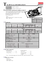
Page 181: ...5 CIRCUIT DIAGRAMS 181 266 Art No 80116 201 09 2004 ICC 200 300 350 CPU PCB bare 40128 026...

Page 182: ...100R R23 18k R22 4k7 R15 3k3 R14 470R R38 4k7 R18 470R R36 36k R35 22k R42 100R R44 1k R33 30k R34 10k R29 470R R31 9k1 R30 4k7 R20 2k2 R28 36k R27 22k R48 4k7 R25 30k R26 10k R50 220R R19 2k2 R49 5k...

Page 183: ...CV TRG THD DCH RES IC5 OUT NE555 CV TRG THD DCH RES IC7 OUT NE555 1D R C1 40174 IC9 J1 J2 J3 MP1 MP2 MP3 R1 10k R10 5k1 R11 51k R16 100k R2 10k R21 n best R24 10k R3 10k R37 2k2 R39 5k1 R4 100k R5 10...

Page 184: ...D DCH RES IC5 OUT NE555 CV TRG THD DCH RES IC7 OUT NE555 1D R C1 40174 IC9 J1 J2 J3 MP1 MP2 MP3 R1 10k R10 5k1 R11 51k R16 100k R2 10k R21 n best R24 10k R3 10k R37 2k2 R39 5k1 R4 100k R5 10k R6 100k...

Page 185: ...RX CX 4528 S R IC21 4013 C D S R IC21 4013 C D IC17 CX R RX CX 4528 IC17 CX R RX CX 4528 IC4 LM319 GND IC9 LM319 IC14 LM319 GND IC16 CX R RX CX 4528 IC16 CX R RX CX 4528 IC14 LM319 GND IC14 LM319 MP1...

Page 186: ...IC1 TL084 IC1 TL084 IC2 LM324 DGND Fout RT CT CT Vin U F IC15 AD654 IC12 4030 1 IC12 4030 1 IC12 4030 1 IC1 TL084 MP5 MP3 R55 1k R47 1k R38 4k7 R43 4k7 R62 4k7 R66 3k9 R23 2k R22 2k R24 2k R21 2k R5 1...

Page 187: ...C2 CS_DFF1 CS_DFF1 CS_DFF1 CS_DFF2 CS_DFF2 CS_DFF2 HF_EIN HF_EIN RESET RESET RESET RESET STE_EIN STE_EIN A AN ANALOG_1 ANALOG_2 ANALOG_3 ANALOG_4 ANALOG_4 AUS B BER_1 BER_1 BER_2 BER_2 DAC_A0 DAC_A1 F...

Page 188: ...188 266 5 CIRCUIT DIAGRAMS ICC 200 300 350 Control board bare 40128 095...

Page 189: ...IC2 1 4049 IC2 1 4049 IC2 1 4049 IC2 1 4049 IC2 1 4049 IC2 1 4049 IC3 1 4049 IC3 1 4049 IC3 1 4049 IC3 1 4049 IC3 1 4049 IC3 1 4049 IC4 4081 IC4 4081 IC4 4081 IC4 4081 J1 J2 J3 MP1 MP2 R2 2k2 R1 2k2 R...

Page 190: ...190 266 5 CIRCUIT DIAGRAMS ICC 200 300 350 QC Power Stage bare 40128 127...

Page 191: ...R12 330R R7 470k R8 200k R1 3R3 R2 30k R3 51k R19 3R3 R16 1k REL1 REL1 REL1 T1 IRFP450 T2 IRFP450 T3 BUZ74 UE2 1 2 3 UE1 1 2 30128 044 30121 073 UE3 1 2 GND GND GND GND GND GND GND GND GND GND GND GND...

Page 192: ...192 266 5 CIRCUIT DIAGRAMS ICC 200 300 350 Power Module bare Power Module UL bare 40128 117...

Page 193: ...9 Q10 Q11 Q12 Q13 Q14 R CLK IC1 4020 IC7 ULN2004A 7667 IC4 7667 IC4 J1 J3 J2 J14 J4 J5 J6 J7 L1 MP3 MP1 R1 4k7 R2 4k7 R3 10R REL1 REL2 REL3 REL3 REL3 REL2 REL2 REL1 REL1 REL19 REL19 REL19 RN2 8x10k RN...

Page 194: ...194 266 5 CIRCUIT DIAGRAMS ICC 200 300 350 ST Power Stage bare 40128 129...

Page 195: ...8 D22 1N4148 D33 15V IC3 LM319 GND IC3 LM319 IC3 LM319 GND IC8 TL084 IC8 TL084 IC8 TL084 IC8 TL084 IC4 AD844 TZ OFF IC7 AD844 TZ OFF IC8 TL084 IC9 TL084 J2 J1 J3 J5 J8 J10 J9 J7 MP1 R50 10k R61 4k7 R5...

Page 196: ...C26 3u3 C25 1uF C23 2n2 C24 10nF C7 1uF C6 1uF C10 18pF C9 18pF C5 10nF C8 1nF D1 15V D2 15V D15 1N4148 D25 3V D4 1N4148 D6 1N4148 D3 9V1 D5 9V1 IC2 TL082 IC2 TL082 RCX CX Q Q IC1 AST TRIG TRIG RTRIG...

Page 197: ...6 4k7 R72 10k R71 10k R73 100R R26 10k R27 1k R56 3k R18 2k4 R29 150R R19 2k4 R60 1k R30 10k R31 5k6 R44 5k6 R45 1k R46 10k R59 30k R68 10k R69 10k R70 10k R41 4k7 R28 2k4 REL1 REL3 REL2 RN1 8x10k T4...

Page 198: ...198 266 5 CIRCUIT DIAGRAMS ICC 200 300 350 Senso board bare 40128 130...

Page 199: ...28 118 30128 479 30128 479 ICC Upper Wiring Module 17 05 95 17 05 95 M Hagg Diese Zeichnung ist urheber ohne unsere Genehmigung Benennung Title Zeichnungsnummer DWG NO Gert UNIT Weitergabe und Verviel...

Page 200: ...200 266 5 CIRCUIT DIAGRAMS ICC 200 300 350 Upper Wiring Module bare 40128 118...

Page 201: ...PCBs only for ICC 200...

Page 202: ...202 266 5 CIRCUIT DIAGRAMS...

Page 203: ...4V PSD0 PSD1 PSD2 PSD3 PSD4 PSD5 PSD6 PSD7 REL NT RES ANA1 RES ANA2 RESET SET SICHER TEMP TEMP TSI TSI TSI STE TSI STE U FUNKE U INP U INP U INT U INT U NESSY U NETZT U NETZT U PHASE U PRIM U PRIM U S...

Page 204: ...ESD2 ESD2 ESD3 ESD3 ESD4 ESD4 ESD5 ESD5 ESD6 ESD6 ESD7 ESD7 FING A1 FING A3 FING B1 FING B3 GND GND GND GND GND GND GND GND GND IP PAT IP PAT A 24V 24V 24V 24V PSD0 PSD1 PSD2 PSD3 RELAIS RES ANA1 RES...

Page 205: ...Name nderung Nr 5 ICC 200 40128 025 30128 033 30128 033 Motherboard 200 M Fritz 25 05 92 B RN18 2k2 8 93 MF 0 5 0 5 0 5 BR1 BH37933 BR2 B250C5000 C6 680uF C7 680uF C15 1000uF C5 u68 C11 68nF C22 68nF...

Page 206: ...1D R C1 40174 IC3 IC7 ULN2004A IC8 ULN2004A IC9 ULN2004A R10 2k2 RN5 8 4k7 RN6 8 10k RN7 8 10k RN12 8 10k RN13 8 10k RN14 8 10k HF EIN RESET SICHER STE EIN CS13 CS14 ESD0 ESD1 ESD2 ESD3 ESD4 ESD5 ESD...

Page 207: ...4050 IC1 1 4050 IC1 1 4050 IC1 1 4050 IC1 1 4050 IC1 1 4050 J24 J23 J25 R11 680R R17 680R R16 680R R12 680R R15 680R R14 680R R13 680R R18 680R R19 680R RN10 8 10k RN3 8 10k RN18 2k2 RN17 8 10k RN11...

Page 208: ...208 266 5 CIRCUIT DIAGRAMS ICC 200 Motherboard bare 40128 025...

Page 209: ...4 1N4148 D6 1N4148 D7 1N4148 D9 SD101A D10 SD101A D1 BA159 D5 11V SFH350 IC1 IC1 SFH450 4047 RCX CX Q Q IC2 AST TRIG TRIG RTRIG MR RX AST OSC OUT G IC3 CX R RX CX 4528 IC3 CX R RX CX 4528 IC5 4011 IC5...

Page 210: ...210 266 5 CIRCUIT DIAGRAMS ICC 200 Mono Output bare 40128 096...

Page 211: ...PCBs only for ICC 300...

Page 212: ...212 266 5 CIRCUIT DIAGRAMS...

Page 213: ...PSD1 PSD2 PSD3 PSD4 PSD5 PSD6 PSD7 REL NT RES ANA1 RES ANA2 RESET SET SICHER TEMP TEMP TSI TSI TSI STE TSI STE U FUNKE U INP U INP U INT U INT U NESSY U NETZT U NETZT U PHASE U PRIM U PRIM U SYM UP HF...

Page 214: ...5 6 CS1 CS10 CS10 CS11 CS11 CS12 CS13 CS2 CS3 CS4 CS5 CS6 CS7 CS8 CS8 CS9 CS9 RESET RESET RESET CS CS13 CS14 ESD0 ESD0 ESD1 ESD1 ESD2 ESD2 ESD3 ESD3 ESD4 ESD4 ESD5 ESD5 ESD6 ESD6 ESD7 ESD7 FING A1 FIN...

Page 215: ...tum Name nderung Nr M Fritz Motherboard A 40128 092 20 07 94 5 20 07 94 M Hagg 30128 394 30128 394 ICC300 0 5 0 5 0 5 BR1 BH37933 BR2 B250C5000 C6 680uF C7 680uF C15 1000uF C5 u68 C11 68nF C22 68nF C9...

Page 216: ...R C1 40174 IC3 IC7 ULN2004A IC8 ULN2004A IC9 ULN2004A R10 2k2 RN5 8 4k7 RN6 8 10k RN7 8 10k RN12 8 10k RN13 8 10k RN14 8 10k HF EIN RESET SICHER STE EIN CS13 CS14 ESD0 ESD1 ESD2 ESD3 ESD4 ESD5 ESD6 ES...

Page 217: ...050 IC1 1 4050 IC1 1 4050 IC1 1 4050 J24 J23 J25 R11 680R R17 680R R16 680R R12 680R R15 680R R14 680R R13 680R R18 680R R19 680R R20 0R RN10 8 10k RN3 8 10k RN18 8 2k2 RN17 8 10k RN11 8 10k RN4 8 10k...

Page 218: ...218 266 5 CIRCUIT DIAGRAMS ICC 300 Motherboard bare 40128 092...

Page 219: ...C3 D 4013 C S R IC3 D 4013 C S R IC7 D 4013 C S R IC7 D 4013 C J2 J3 J4 J1 MP1 R15 10k R14 10k R13 4k7 R17 4k7 R7 510R R8 680R R2 150R R1 56R R3 0R R20 5k1 R16 4k7 R18 4k7 R9 510R R10 680R R6 150R R5...

Page 220: ...220 266 5 CIRCUIT DIAGRAMS ICC 300 Relay Board bare 40128 093...

Page 221: ...PCBs only for ICC 350...

Page 222: ...222 266 5 CIRCUIT DIAGRAMS...

Page 223: ...D1 PSD2 PSD3 PSD4 PSD5 PSD6 PSD7 REL NT RES ANA1 RES ANA2 RESET SET SICHER TEMP TEMP TSI TSI TSI STE TSI STE U FUNKE U INP U INP U INT U INT U NESSY U NETZT U NETZT U PHASE U PRIM U PRIM U SYM UP HF U...

Page 224: ...ESD5 ESD5 ESD6 ESD6 ESD6 ESD7 ESD7 ESD7 FING A1 FING A2 FING A3 FING B1 FING B2 FING B3 GND GND GND GND GND GND GND GND GND IP PAT IP PAT A 24V 24V 24V 24V PSD0 PSD1 PSD2 PSD3 RES ANA1 RES ANA2 RES B...

Page 225: ...atum Name nderung Nr M Fritz ICC 6 Motherboard A 27 01 94 40128 092 30128 351 30128 351 20 07 94 M Hagg 0 5 0 5 0 5 BR1 BH37933 BR2 B250C5000 C6 680uF C7 680uF C15 1000uF C5 u68 C11 68nF C22 68nF C9 6...

Page 226: ...C1 40174 IC3 IC7 ULN2004A IC8 ULN2004A IC9 ULN2004A R10 2k2 RN5 8 4k7 RN6 8 10k RN7 8 10k RN12 8 10k RN13 8 10k RN14 8 10k HF EIN RESET SICHER STE EIN CS13 CS14 ESD0 ESD1 ESD2 ESD3 ESD4 ESD5 ESD6 ESD7...

Page 227: ...IC1 1 4050 IC1 1 4050 IC1 1 4050 IC1 1 4050 J24 J23 J25 R11 680R R17 680R R16 680R R12 680R R15 680R R14 680R R13 680R R18 680R R19 680R RN10 8 10k RN3 8 10k RN18 8 2k2 RN17 8 10k RN11 8 10k RN4 8 10k...

Page 228: ...128 351 20 07 94 M Hagg C13 10nF C12 68nF C14 68nF C28 u15 C31 u022 C30 u022 C29 u15 C26 68nF C27 68nF C25 1uF D5 1N4148 D6 10V D7 10V D10 BA159 D11 BA159 D12 1N4148 D9 1N4148 D22 1N4148 rot D23 D24 B...

Page 229: ...5 CIRCUIT DIAGRAMS 229 266 Art No 80116 201 09 2004 ICC 350 Motherboard bare 40128 092...

Page 230: ...S R IC3 D 4013 C S R IC7 D 4013 C S R IC7 D 4013 C J2 J3 J4 J1 MP1 R15 10k R14 10k R13 4k7 R17 4k7 R7 510R R8 680R R2 150R R1 56R R3 0R R20 5k1 R16 4k7 R18 4k7 R9 510R R10 680R R6 150R R5 56R R4 0R R2...

Page 231: ...5 CIRCUIT DIAGRAMS 231 266 Art No 80116 201 09 2004 ICC 350 Relay Board bare 40128 093...

Page 232: ...GND Fout RT CT CT Vin U F IC4 AD654 IC3 TL082 IC3 TL082 IC3 TL082 IC6 TL082 J1 J2 J4 J5 MP5 MP3 MP2 MP6 MP4 MP1 MP9 R1 820k R4 220R R9 10k R12 390R R23 10k R13 10k R22 220k R15 10k R3 1k R5 470R R38 8...

Page 233: ...D16 1N4148 rot D14 1D R C1 40174 IC14 IC13 ULN2004A IC8 CNY66 IC9 CNY66 IC10 CNY66 IC11 CNY66 IC12 CNY66 IC7 CNY66 IC6 TL082 IC6 TL082 0 1 2 3 4 5 6 7 8 9 1 2 4 8 IC5 BCD DEC 4028 MP7 R31 1k3 R32 1k3...

Page 234: ...234 266 5 CIRCUIT DIAGRAMS ICC 350 Neurotest Neurotest Board 40128 027...

Page 235: ...J3 J4 J2 L1 1m8 R1 100R R7 100R R2 1k R3 1k R5 22k R4 10k R6 1k T1 BC517 UE1 10 10 1 2 CS11 CS12 CS12 CS13 CS13 RESET RESET ESD0 ESD0 ESD1 ESD1 ESD2 ESD2 ESD3 ESD3 ESD4 ESD4 ESD5 ESD5 ESD6 ESD6 ESD7...

Page 236: ...236 266 5 CIRCUIT DIAGRAMS ICC 350 Neurotest Motherboard Neurotest bare 40128 028...

Page 237: ...R22 10k R21 10k R19 10k R18 22k R16 5k6 R29 2k4 R30 2k4 R14 2k4 R15 2k R13 390R R17 2k4 R28 2k4 R23 10k R31 22k R7 4k7 R8 4k7 R32 4k7 R33 2k7 R34 4k7 R35 2k7 REL1 REL1 REL6 REL6 REL1 REL6 REL7 REL7 R...

Page 238: ...238 266 5 CIRCUIT DIAGRAMS ICC 350 MIC MIEN DOKU MIC Board bare 40128 064...

Page 239: ...g Title Zeichnungsnummer DWG NO Gert UNIT Weitergabe und Vervielfltigung rechtlich gesch tzt daher unzulssig Datum Name Gezeich Gepr ft LP un LP bs Blatt von Datum Name nderung A Nr ICC 350 MMH Doku 1...

Page 240: ...240 266 5 CIRCUIT DIAGRAMS ICC 350 MIC MIEN DOKU Protection Board bare 40128 141...

Page 241: ...AppendixA Part Numbers...

Page 242: ......

Page 243: ...2004 ICC 200 D 10128 002 010 023 30128 060 40128 103 50502 059 30121 195 51501 167 30121 025 30128 065 30121 023 30128 056 51501 167 30121 086 51611 051 Fuses 51603 000 cpl 51601 056 50610 009 51031 0...

Page 244: ...02 204 205 30128 458 40128 103 50502 069 30128 728 51501 167 30128 065 30128 727 30128 056 51501 167 30121 086 51603 000 cpl 51601 056 50610 009 51031 043 51501 190 51501 191 51501 192 30128 063 30128...

Page 245: ...200 INT 10128 009 015 036 30128 458 40128 103 50502 059 30128 728 51501 167 30128 065 30128 727 30128 056 51501 167 30121 086 51611 051 Fuses 51603 000 51601 056 50610 009 51031 043 Pot 51501 190 But...

Page 246: ...200 F 10128 051 054 056 30128 116 40128 112 50502 059 30121 195 51501 167 30121 025 30128 065 30121 023 30128 056 51501 167 30121 086 51611 051 51603 000 51601 056 50610 009 51031 043 51501 190 51501...

Page 247: ...80116 201 09 2004 ICC 200 Boards 40128 103 40128 112 F Gezeich Drawn Gepr ft Checked Freigabe Approv Datum Date Name Name Ma stab Scale Datei File Projekt Project Benennung Title Nummer Number Ers f r...

Page 248: ...10128 070 071 30121 086 30127 011 30128 022 50610 009 51601 025 51611 051 Fuse 51603 000 51031 043 Pot 51501 190 191 192 51501 167 50502 059 30121 025 40128 133 30121 023 30121 023 30121 390 30121 195...

Page 249: ...4 ICC 300 UL 10128 213 214 30121 086 30127 011 30128 022 50610 009 51601 025 51611 100 Fuses 51031 043 51501 190 191 192 50502 069 40128 133 30128 726 30121 390 30128 728 51501 167 30128 021 30128 419...

Page 250: ...NT 10128 077 078 30121 086 30127 011 30128 022 50610 009 51601 025 51611 051 Fuse 51603 000 51031 043 51501 190 191 192 50502 059 30128 691 40128 133 30128 726 30121 390 30128 728 51501 167 30128 021...

Page 251: ...09 2004 ICC 300 F 10128 072 073 51501 167 50502 059 30121 025 40128 134 30121 023 30121 023 30121 390 30121 195 51501 167 30128 021 30128 315 30121 086 30127 011 30128 022 50610 009 51601 025 51611 05...

Page 252: ...66 ICC 300 Boards 40128 133 D INT 40128 134 F Gezeich Drawn Gepr ft Checked Freigabe Approv Datum Date Name Name Ma stab Scale Datei File Projekt Project Benennung Title Nummer Number Ers f r Replaces...

Page 253: ...ICC 350 D 10128 016 Endo 50502 059 40128 101 30128 016 30121 390 30121 025 30121 023 30121 023 30121 195 30128 021 51601 025 51501 167 51501 167 30121 086 30127 011 51603 000 30128 022 50610 009 5103...

Page 254: ...0128 200 206 Endo 51603 000 51501 167 30121 086 30127 011 30128 022 50610 009 51031 043 51501 190 51501 191 51501 192 51611 100 Fuses 50502 069 40128 101 30128 441 30121 390 30128 726 30128 728 30128...

Page 255: ...ICC 350 INT 10128 061 Endo 50502 059 40128 101 30128 441 30121 390 30128 726 30128 728 30128 021 30128 691 30128 725 51601 025 51501 167 51501 167 30121 086 30127 011 51603 000 30128 022 50610 009 510...

Page 256: ...110 30128 080 30128 679 MIC 30121 390 30121 025 30121 023 30121 023 30121 195 30128 021 30128 668 51501 167 51501 167 30121 086 30127 011 51603 000 30128 022 30128 680 MIC 50610 009 51031 043 51501 1...

Page 257: ...oku 10128 081 50502 059 40128 101 30128 533 30121 390 30121 025 30121 023 30121 023 30121 195 30128 021 30128 668 50600 021 51501 167 30121 086 51708 043 30127 011 51601 025 50610 009 51611 051 51603...

Page 258: ...50502 059 40128 101 30128 083 30121 390 30121 025 30121 023 30121 023 30121 195 30128 021 51501 167 51501 167 30121 086 30127 011 51603 000 30128 085 50610 009 51031 043 51501 190 51501 191 51501 192...

Page 259: ...C 350 T 10128 066 50502 059 40128 101 30128 089 30121 390 30121 025 30121 023 30121 023 30121 195 30128 021 51501 167 30121 086 30127 011 51604 035 51603 000 30128 085 50610 009 51031 043 51501 190 51...

Page 260: ...310 50502 059 40128 101 30128 606 30121 390 30128 726 30128 728 30128 021 30128 668 51501 167 30121 086 51708 043 30127 011 51601 025 50610 009 51611 051 51603 000 51501 167 51031 043 51501 190 51501...

Page 261: ...350 M 10128 080 50502 059 40128 101 30128 533 30121 390 30121 025 30121 023 30121 023 30121 195 30128 021 30128 668 51501 167 30121 086 51708 043 30127 011 51601 025 50610 009 51611 051 51603 000 5150...

Page 262: ...2 266 ICC 350 Boards 40128 101 40128 110 F Gezeich Drawn Gepr ft Checked Freigabe Approv Datum Date Name Name Ma stab Scale Datei File Projekt Project Benennung Title Nummer Number Ers f r Replaces Er...

Page 263: ...Appendix B Abbreviations Notes Addresses...

Page 264: ...264 266 B APPENDIX B...

Page 265: ...ms of electrical dimensions The diagrams of the electrical dimensions are not shown in this service manual However you will find these printed in the instruction manuals for the respective unit Any qu...

Page 266: ...Your notes...

Reviews: