EDM01-33v1 DAG_7.5G4_Card_User_Guide
4
©2008 Endace Technology Ltd. Confidential - Version 1 - November 2008
Card Architecture
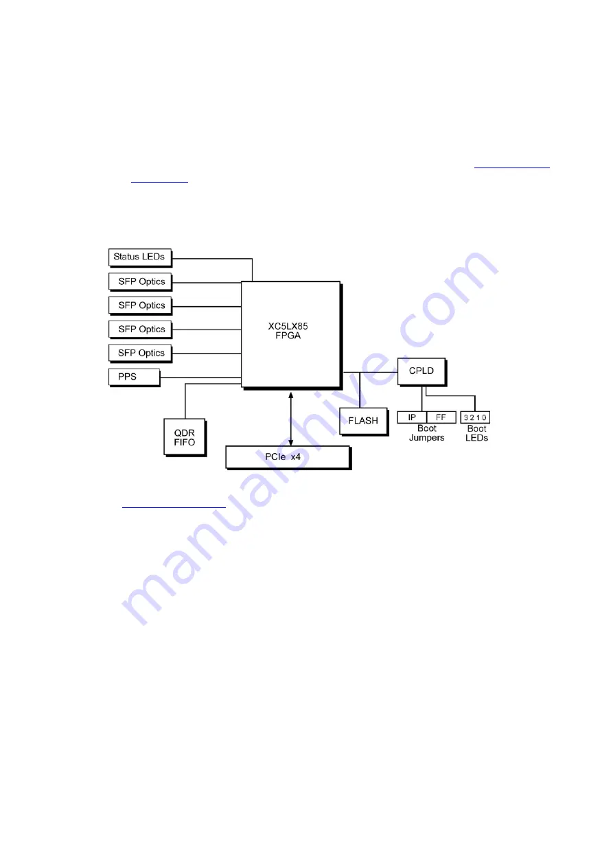
Serial Ethernet network data received by each 1000Base interface flows directly into the Field
Programmable Gate Array (FPGA).
The FPGA contains the packet processor, PCIe interface logic and the DAG Universal Clock
Kit (DUCK) timestamp engine. The DUCK provides high resolution per-packet timestamps
which can be accurately synchronized.
Note:
For further information on the DUCK and time synchronization, see
Synchronizing
Clock Time
(page ) later in this user guide.
Because of component close association, packets are time-stamped accurately. Time stamped
packet records are stored in an external FIFO memory before transmission to the host.
The diagram below shows the DAG 7.5G4G4 card's major components and flow of data.
For more information about the Boot jumpers and LEDs see:
•
Boot jumper settings
(page )
•
Boot LEDs
Summary of Contents for DAG 5.2X
Page 1: ...DAG 7 5G4 Card User Guide EDM01 33...
Page 12: ......
Page 18: ......
Page 64: ......
Page 66: ......


